MX-5050BII Instruction Manual — Digital Edition · Part 10 · scan pages 111-116
Circuit Diagrams
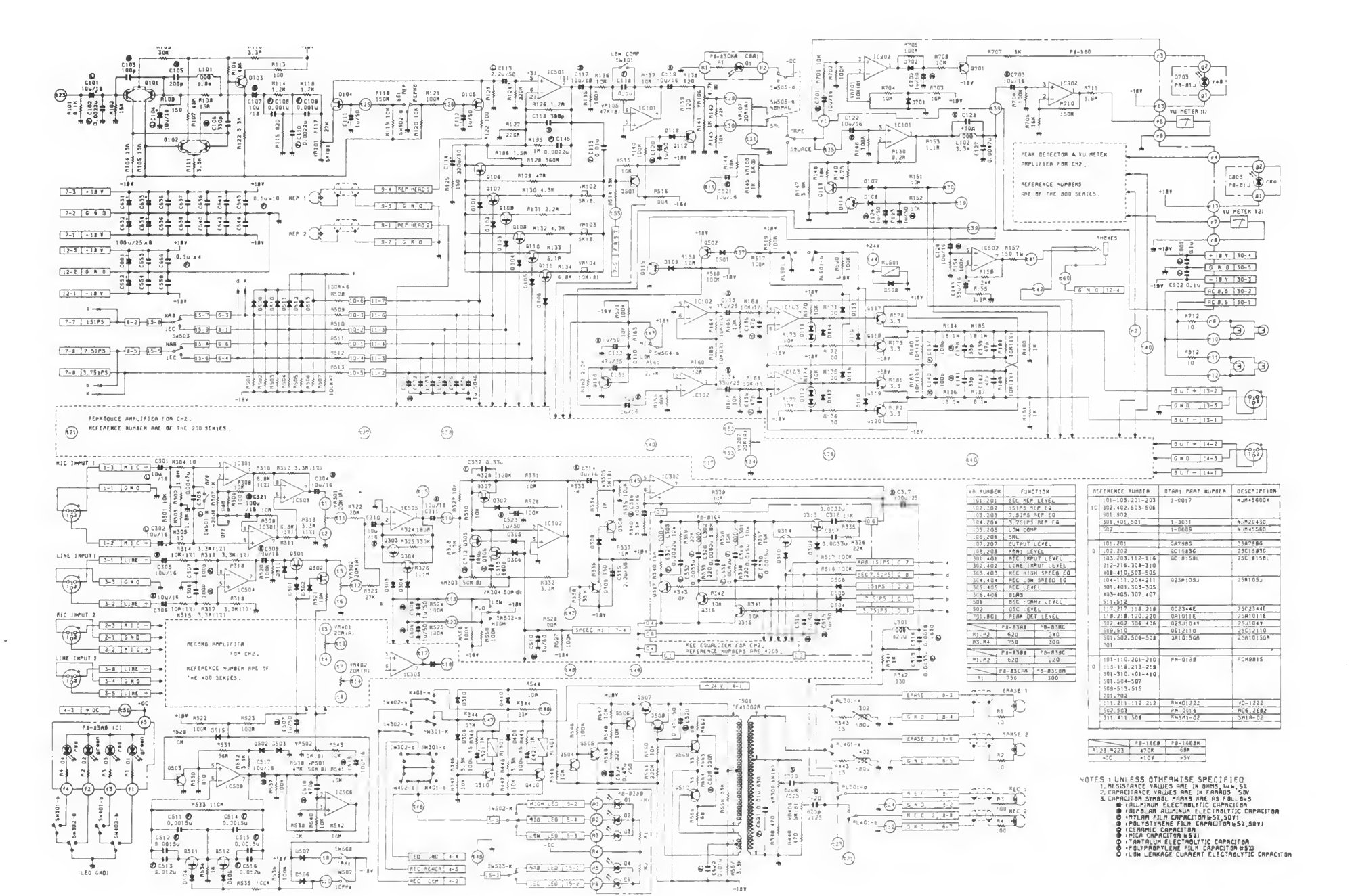 ⤢ zoomFull schematic of the A10620B record and reproduce amplifier channel board, with the mic and line inputs, equalizer, bias oscillator and output stages.
Full-resolution scan of this sheet
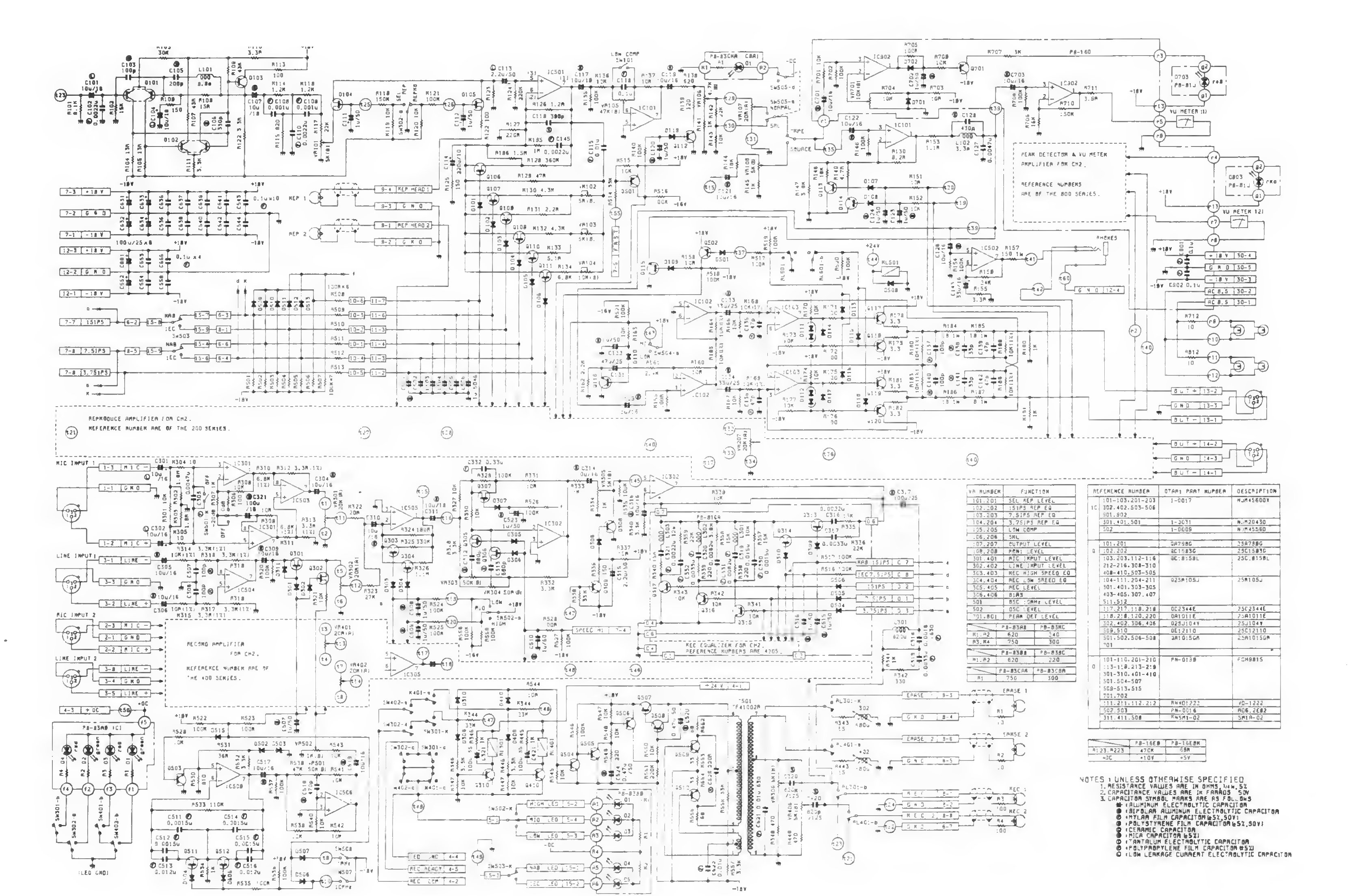
A10620B REC & REPRO AMP.
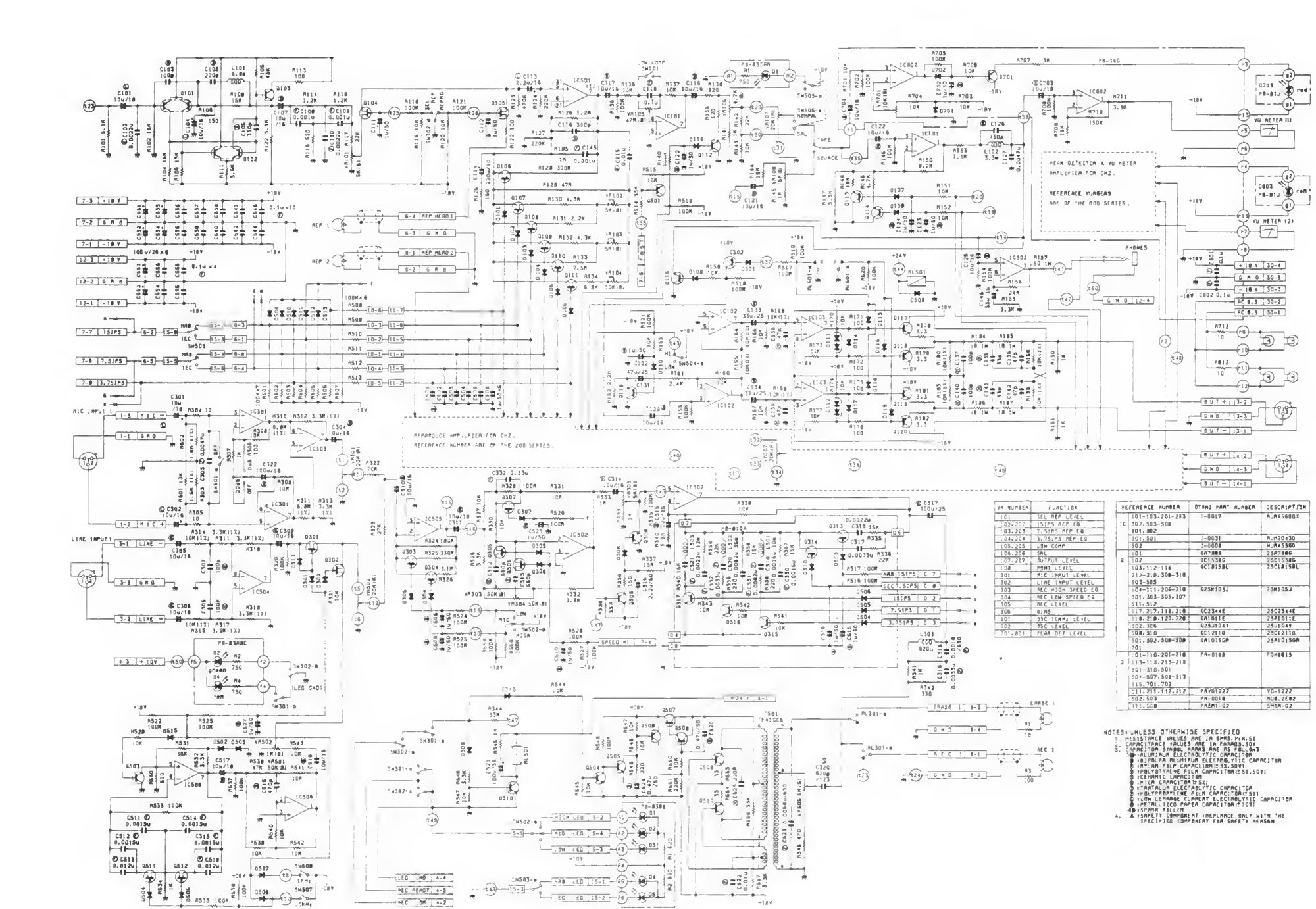 ⤢ zoomFull schematic of the A10680C record and reproduce amplifier channel board, labelled for channel 2: mic and line inputs, the reproduce amplifier, and the peak detector and VU meter amplifier.
Full-resolution scan of this sheet
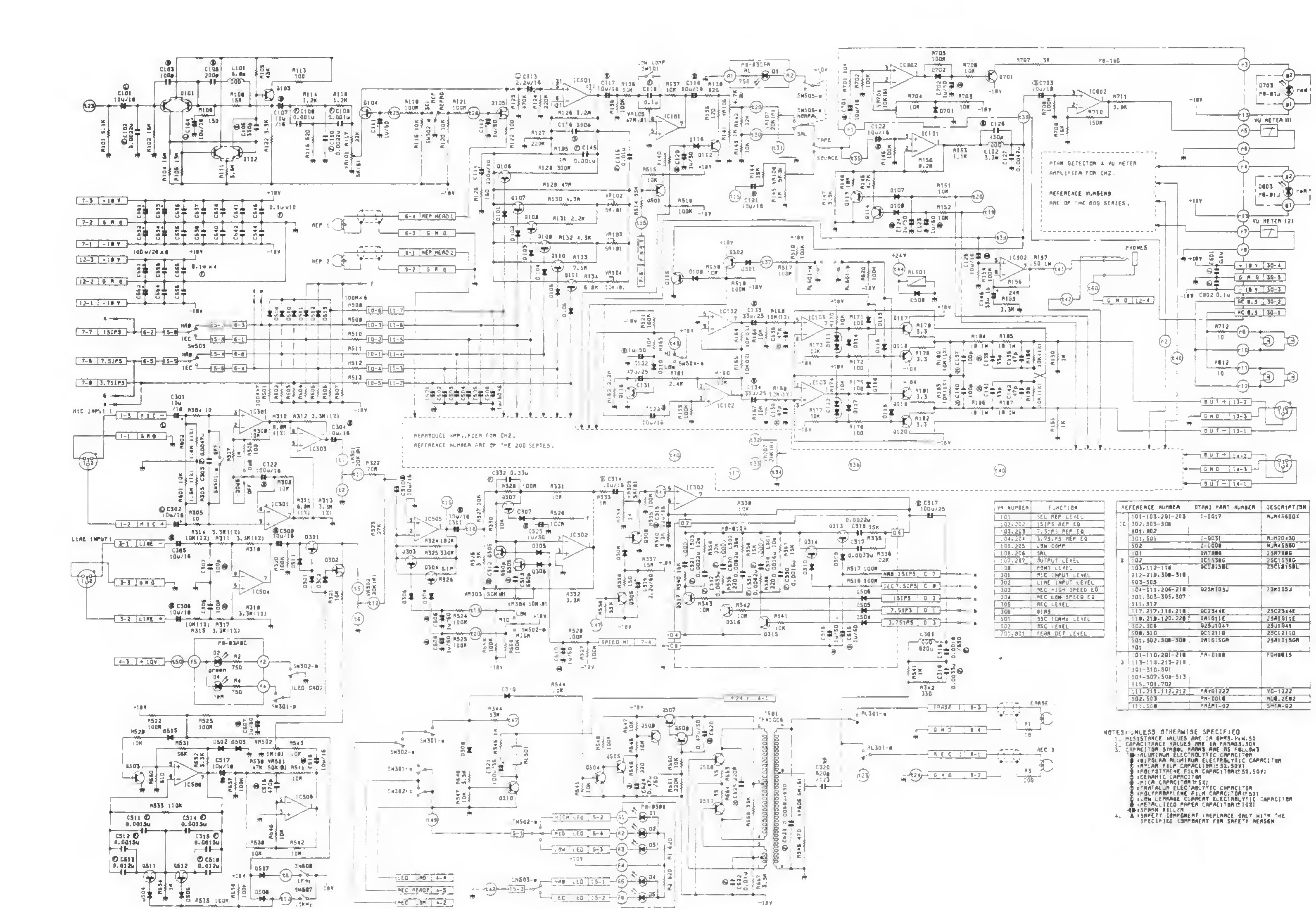
A10680C REC & REPRO AMP.
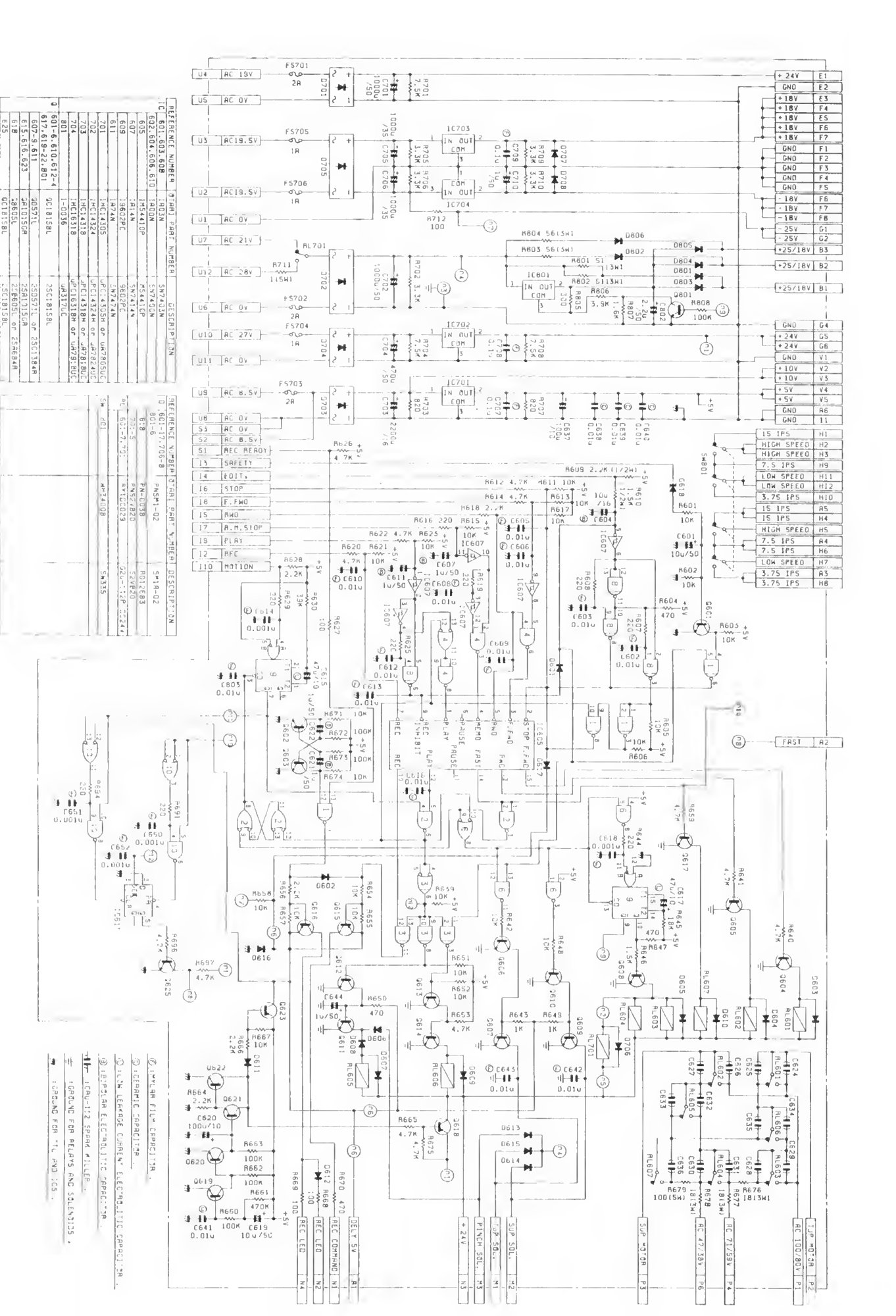 ⤢ zoomFull schematic of the PB-46Q control P.C.B., with the connector pinouts and transport mode logic.
Full-resolution scan of this sheet
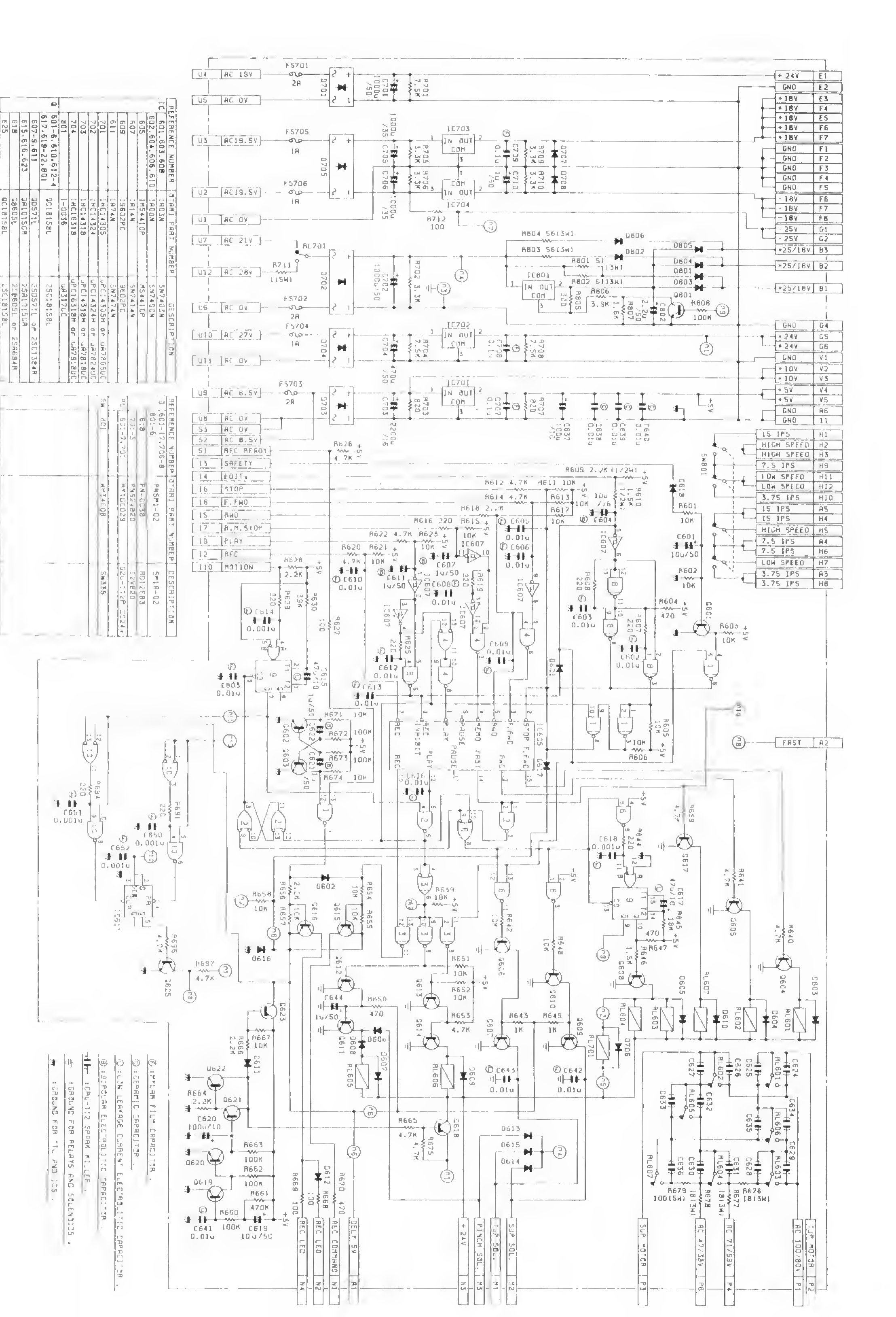
PB-46Q CONTROL P.C.B. ASSEMBLY
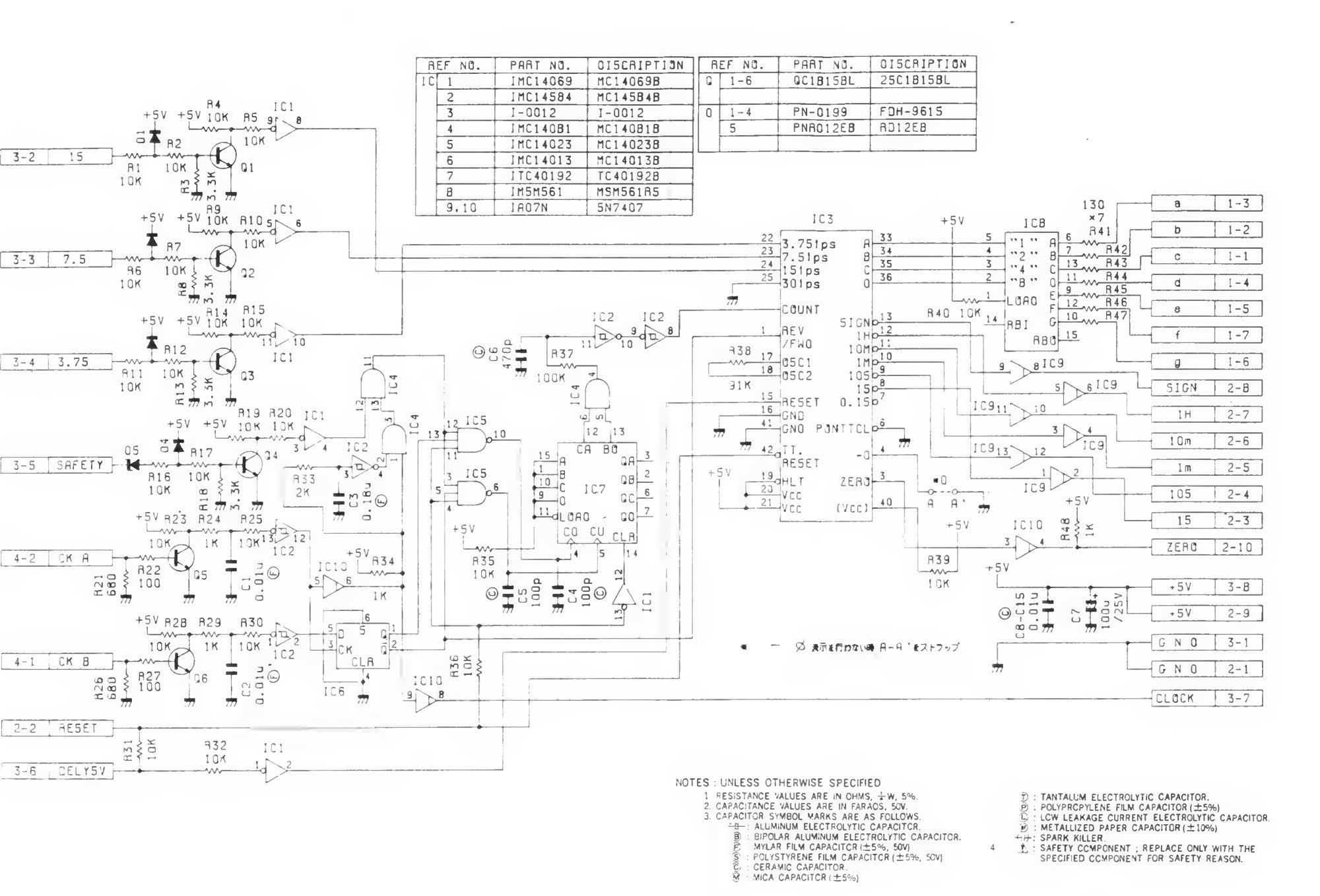 ⤢ zoomFull schematic of the PB-46R timer drive P.C.B., with the counter, display driver and oscillator circuits.
Full-resolution scan of this sheet
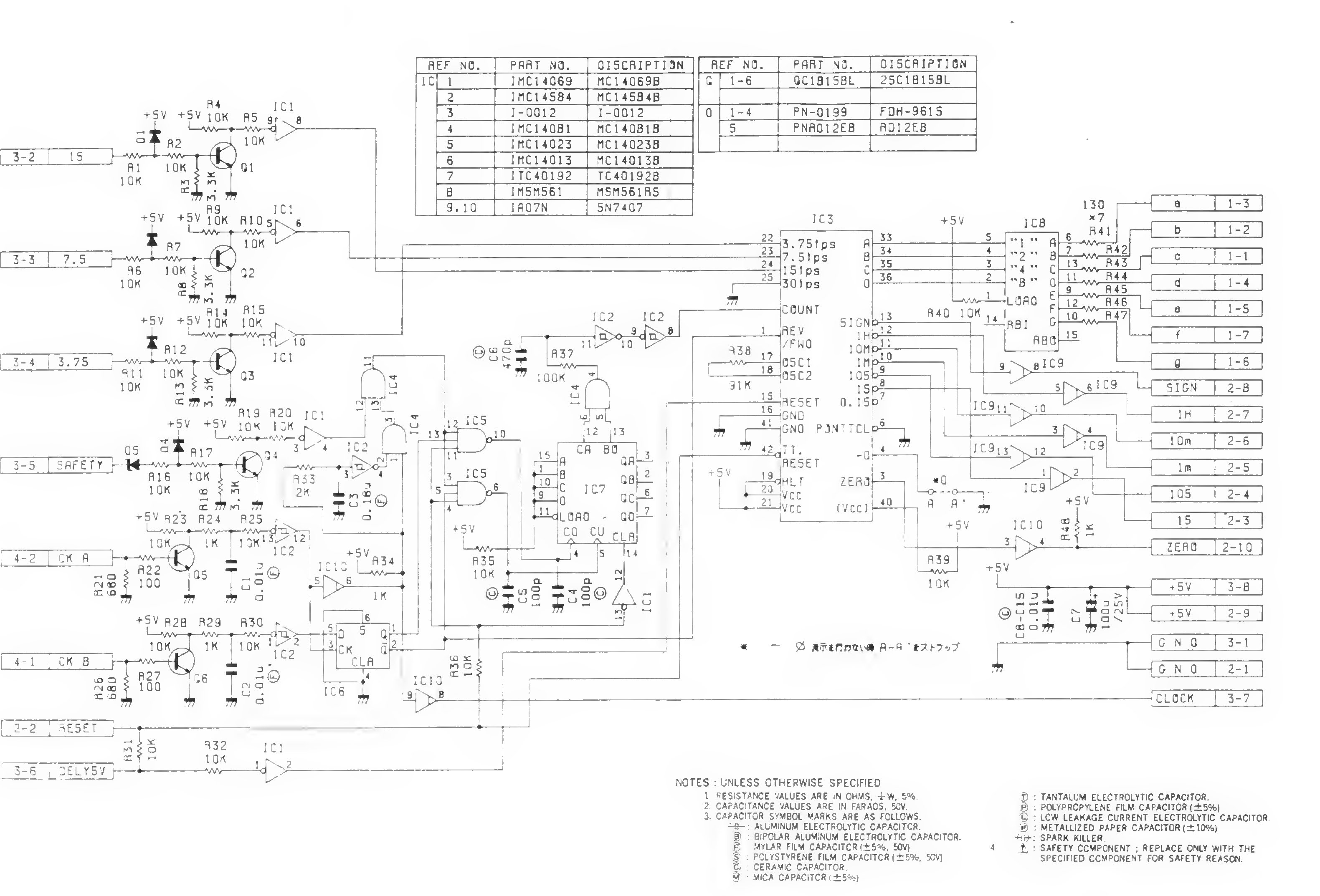
PB-46R TIMER DRIVE P.C.B. ASSEMBLY
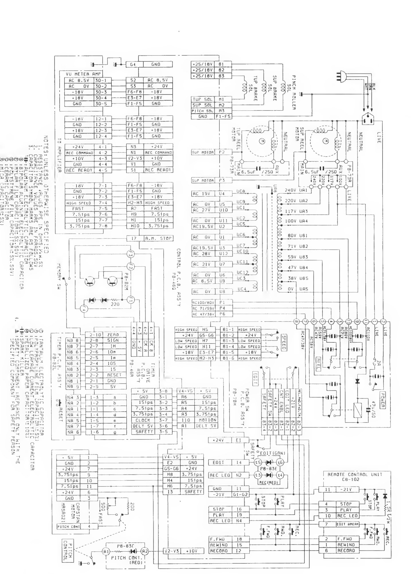 ⤢ zoomWiring diagram for the transport, showing the power supply, motors, solenoids, and the control and timer boards and their interconnections.
Full-resolution scan of this sheet
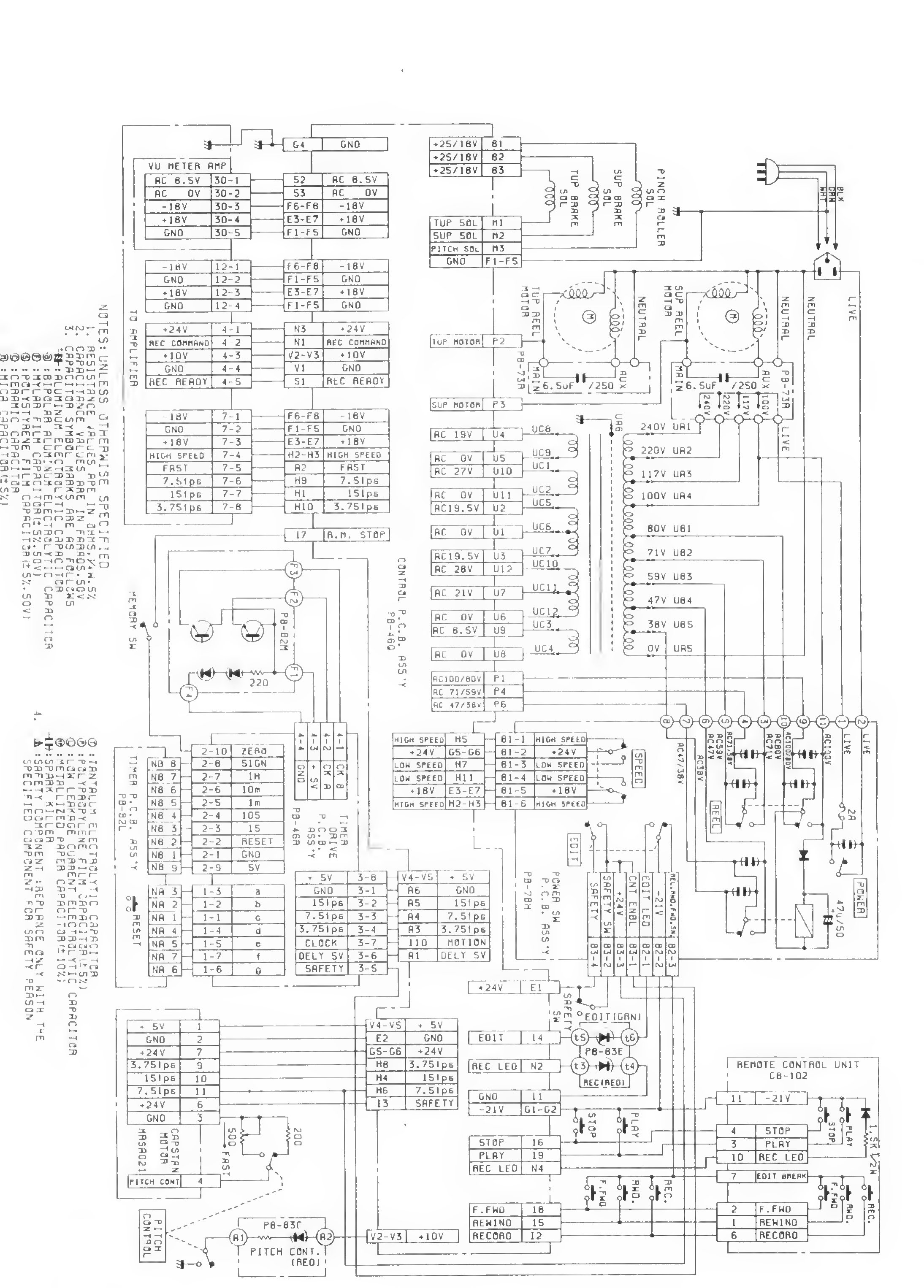
WIRING DIAGRAM TRANSPORT