BQ-II manual, Section 10 · Site-authored simulation
Simulating the AMP control board
The BQ-II's AMP control P.C.B. (PB45E0A, Otari drawing 3-6649) carries the record command logic, the two 555 clocks, the 1 kHz and 10 kHz test oscillators, the EQ select buffer and the power-on mute. This site redrew the sheet in KiCad 10 at Otari's positions and ran it in ngspice: five scenarios and 226 checks, each against an expected value or range, most worked out from the parts on the drawing and the rest logic levels, datasheet typicals and sanity bounds. This is a simulation of Otari's drawing, not of a physical board.
The redrawn sheet (SVG) · PDF · KiCad project (zip) · the scan in Section 10. Exported with KiCad 10.0.4.
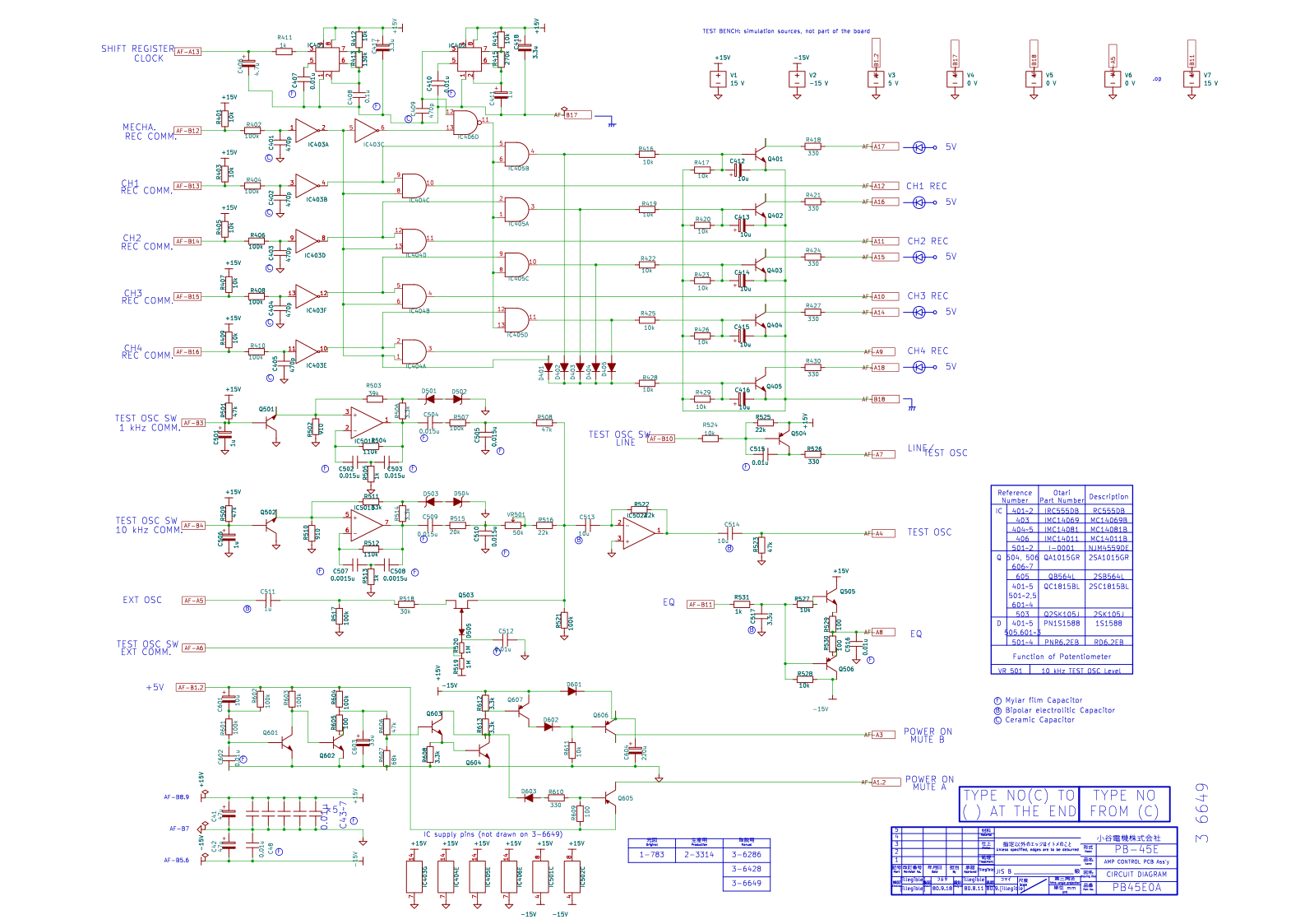
Bench
What the simulation adds around the board, where the drawing stops:
- The sheet's bench: +15 V, -15 V and +5 V (P5V) supplies; AF-B17 and AF-B18 grounded off-board; EXT OSC IN (AF-A5) at 0 V; EQ select (AF-B11) at +15 V, the Control PCB's low-speed state.
- Switches to ground (MECHA REC COMM, CH1-CH4 REC, TEST OSC 1 kHz / 10 kHz, EXT OSC, LINE) are 0 V sources; an open switch leaves the pin to its pull-up.
- REC LEDs (AF-A14 .. A18): a generic red LED from MUTE A (P.O.M.A) to each pin, in scenarios 2 and 4. The Mother PCB (3-6287) feeds the front panel's REC LED from P.O.M.A (AM3); the LED is off this drawing.
- EXT OSC input: 1 V peak at 400 Hz, in scenario 3.
- Power in scenario 5: the three supplies switch on as a step at 0 s (uic: every capacitor starts empty) and fall together, linearly, to 0 V over 50 ms from 4.0 s (assumed; the real supplies' decay is not on this drawing).
- MUTE A loaded by 1 kohm and MUTE B by 10 kohm to ground, in scenario 5 (assumed; the channel cards' mute inputs are not modelled).
1. DC operating point, idle
| Check | Simulated | Expected | Basis |
|---|---|---|---|
| +15 V supply current | 34.26 mA | 30 to 40 mA | 2 x RC555 (10 mA typ), 2 x NJM4559 (3.5 mA typ), the mute drivers |
| -15 V supply current | 9.747 mA | 8.755 to 10.7 mA | 2 x NJM4559 and R528 |
| +5 V supply current | 8.657 mA | 7 to 11 mA | R609, R610 into Q604 and Q605's base |
| GND B17 return | 21.15 mA | 18 to 24 mA | both RC555s return through AF-B17 |
| IC401 control voltage | 10 V | 9.95 to 10.05 V | 2/3 of VCC |
| Q401 off: collector current | ≈ 0 µA | 0 to 1 µA | |
| Q402 off: collector current | ≈ 0 µA | 0 to 1 µA | |
| Q403 off: collector current | ≈ 0 µA | 0 to 1 µA | |
| Q404 off: collector current | ≈ 0 µA | 0 to 1 µA | |
| Q405 off: collector current | ≈ 0 µA | 0 to 1 µA | |
| Q602 off: collector current | ≈ 0 µA | 0 to 1 µA | |
| Q501 on, oscillator held off: base current | 305.1 µA | 274.6 to 335.6 µA | +15 V through R501 |
| Q502 on, oscillator held off: base current | 305.1 µA | 274.6 to 335.6 µA | +15 V through R509 |
| Q503 (EXT OSC gate) off: drain current | 0.015 nA | 0 to 1 nA | |
| Q504 (LINE) off: base current | ≈ 0 µA | 0 to 1 µA | |
| Q601 on: base current | 22 µA | 18.7 to 25.3 µA | (5 V - VBE) through R602 + R601 |
| Q604 on: collector current | 12.37 mA | 5 to 20 mA | Darlington with Q603 |
| Q605 on (MUTE A at +5 V): base current | 1.777 mA | 1 to 3 mA | |
| Q606 off (MUTE B released): collector current | ≈ 0 µA | 0 to 1 µA | |
| Q607 on: collector current | 1.438 mA | 1.296 to 1.584 mA | into D602 and R611 |
| C603 (mute timer) charged | 2.512 V | 2.3 to 2.7 V | R604 / (R606 + R607) divider less Q603's base |
| EQ OUT at low speed | 12.27 V | 12.15 to 12.39 V | R531 / R528 divider |
AF pins, idle
| AF pin | net | idle (V) |
|---|---|---|
| AF-A1.2 | MUTE_A | 4.994 |
| AF-A10 | CH3_REC | 0.000 |
| AF-A11 | CH2_REC | 0.000 |
| AF-A12 | CH1_REC | 0.000 |
| AF-A13 | SRCLK | 9.678 |
| AF-A14 | LED4 | 0.000 |
| AF-A15 | LED3 | 0.000 |
| AF-A16 | LED2 | 0.000 |
| AF-A17 | LED1 | 0.000 |
| AF-A18 | LED5 | 0.000 |
| AF-A3 | MUTE_B | 14.819 |
| AF-A4 | TEST_OSC | 0.000 |
| AF-A5 | EXT_IN | 0.000 |
| AF-A6 | EXT_SW | -15.000 |
| AF-A7 | LINE_OUT | 15.000 |
| AF-A8 | EQ_OUT | 12.267 |
| AF-A9 | CH4_REC | 0.000 |
| AF-B1.2 | P5V | 5.000 |
| AF-B10 | LINE_SW | 15.000 |
| AF-B11 | EQ_IN | 15.000 |
| AF-B12 | MECHA_IN | 15.000 |
| AF-B13 | CH1_IN | 15.000 |
| AF-B14 | CH2_IN | 15.000 |
| AF-B15 | CH3_IN | 15.000 |
| AF-B16 | CH4_IN | 15.000 |
| AF-B17 | GND_B17 | 0.000 |
| AF-B18 | GND_B18 | 0.000 |
| AF-B3 | OSC1_SW | 0.658 |
| AF-B4 | OSC2_SW | 0.658 |
| AF-B5.6 | -15V | -15.000 |
| AF-B7 | GND | 0.000 |
| AF-B8.9 | +15V | 15.000 |
2. DC operating point per mode
| Check | Simulated | Expected | Basis |
|---|---|---|---|
| idle: CH1 REC COMM low | 0 V | -0.01 to 0.5 V | |
| idle: CH2 REC COMM low | 0 V | -0.01 to 0.5 V | |
| idle: CH3 REC COMM low | 0 V | -0.01 to 0.5 V | |
| idle: CH4 REC COMM low | 0 V | -0.01 to 0.5 V | |
| idle: LED1 off | 0 mA | -0.01 to 0.1 mA | |
| idle: LED2 off | 0 mA | -0.01 to 0.1 mA | |
| idle: LED3 off | 0 mA | -0.01 to 0.1 mA | |
| idle: LED4 off | 0 mA | -0.01 to 0.1 mA | |
| idle: LED5 off | 0 mA | -0.01 to 0.1 mA | |
| MECHA REC: CH1 REC COMM low | 0 V | -0.01 to 0.5 V | |
| MECHA REC: CH2 REC COMM low | 0 V | -0.01 to 0.5 V | |
| MECHA REC: CH3 REC COMM low | 0 V | -0.01 to 0.5 V | |
| MECHA REC: CH4 REC COMM low | 0 V | -0.01 to 0.5 V | |
| MECHA REC: LED1 off | 0 mA | -0.01 to 0.1 mA | |
| MECHA REC: LED2 off | 0 mA | -0.01 to 0.1 mA | |
| MECHA REC: LED3 off | 0 mA | -0.01 to 0.1 mA | |
| MECHA REC: LED4 off | 0 mA | -0.01 to 0.1 mA | |
| MECHA REC: LED5 on | 9.244 mA | 8.335 to 10.19 mA | red LED from MUTE A, 330 ohm |
| MECHA REC + CH1: CH1 REC COMM high | 15 V | 13.5 to 15.01 V | MC14081B AND of MECHA and the channel |
| MECHA REC + CH1: CH2 REC COMM low | 0 V | -0.01 to 0.5 V | |
| MECHA REC + CH1: CH3 REC COMM low | 0 V | -0.01 to 0.5 V | |
| MECHA REC + CH1: CH4 REC COMM low | 0 V | -0.01 to 0.5 V | |
| MECHA REC + CH1: LED1 on | 9.202 mA | 8.294 to 10.14 mA | red LED from MUTE A, 330 ohm |
| MECHA REC + CH1: LED2 off | 0 mA | -0.01 to 0.1 mA | |
| MECHA REC + CH1: LED3 off | 0 mA | -0.01 to 0.1 mA | |
| MECHA REC + CH1: LED4 off | 0 mA | -0.01 to 0.1 mA | |
| MECHA REC + CH1: LED5 on | 9.2 mA | 8.294 to 10.14 mA | red LED from MUTE A, 330 ohm |
| MECHA REC + CH2: CH1 REC COMM low | 0 V | -0.01 to 0.5 V | |
| MECHA REC + CH2: CH2 REC COMM high | 15 V | 13.5 to 15.01 V | MC14081B AND of MECHA and the channel |
| MECHA REC + CH2: CH3 REC COMM low | 0 V | -0.01 to 0.5 V | |
| MECHA REC + CH2: CH4 REC COMM low | 0 V | -0.01 to 0.5 V | |
| MECHA REC + CH2: LED1 off | 0 mA | -0.01 to 0.1 mA | |
| MECHA REC + CH2: LED2 on | 9.202 mA | 8.294 to 10.14 mA | red LED from MUTE A, 330 ohm |
| MECHA REC + CH2: LED3 off | 0 mA | -0.01 to 0.1 mA | |
| MECHA REC + CH2: LED4 off | 0 mA | -0.01 to 0.1 mA | |
| MECHA REC + CH2: LED5 on | 9.2 mA | 8.294 to 10.14 mA | red LED from MUTE A, 330 ohm |
| MECHA REC + CH3: CH1 REC COMM low | 0 V | -0.01 to 0.5 V | |
| MECHA REC + CH3: CH2 REC COMM low | 0 V | -0.01 to 0.5 V | |
| MECHA REC + CH3: CH3 REC COMM high | 15 V | 13.5 to 15.01 V | MC14081B AND of MECHA and the channel |
| MECHA REC + CH3: CH4 REC COMM low | 0 V | -0.01 to 0.5 V | |
| MECHA REC + CH3: LED1 off | 0 mA | -0.01 to 0.1 mA | |
| MECHA REC + CH3: LED2 off | 0 mA | -0.01 to 0.1 mA | |
| MECHA REC + CH3: LED3 on | 9.202 mA | 8.294 to 10.14 mA | red LED from MUTE A, 330 ohm |
| MECHA REC + CH3: LED4 off | 0 mA | -0.01 to 0.1 mA | |
| MECHA REC + CH3: LED5 on | 9.2 mA | 8.294 to 10.14 mA | red LED from MUTE A, 330 ohm |
| MECHA REC + CH4: CH1 REC COMM low | 0 V | -0.01 to 0.5 V | |
| MECHA REC + CH4: CH2 REC COMM low | 0 V | -0.01 to 0.5 V | |
| MECHA REC + CH4: CH3 REC COMM low | 0 V | -0.01 to 0.5 V | |
| MECHA REC + CH4: CH4 REC COMM high | 15 V | 13.5 to 15.01 V | MC14081B AND of MECHA and the channel |
| MECHA REC + CH4: LED1 off | 0 mA | -0.01 to 0.1 mA | |
| MECHA REC + CH4: LED2 off | 0 mA | -0.01 to 0.1 mA | |
| MECHA REC + CH4: LED3 off | 0 mA | -0.01 to 0.1 mA | |
| MECHA REC + CH4: LED4 on | 9.202 mA | 8.294 to 10.14 mA | red LED from MUTE A, 330 ohm |
| MECHA REC + CH4: LED5 on | 9.2 mA | 8.294 to 10.14 mA | red LED from MUTE A, 330 ohm |
| TEST OSC 1 kHz: CH1 REC COMM low | 0 V | -0.01 to 0.5 V | |
| TEST OSC 1 kHz: CH2 REC COMM low | 0 V | -0.01 to 0.5 V | |
| TEST OSC 1 kHz: CH3 REC COMM low | 0 V | -0.01 to 0.5 V | |
| TEST OSC 1 kHz: CH4 REC COMM low | 0 V | -0.01 to 0.5 V | |
| TEST OSC 1 kHz: LED1 off | 0 mA | -0.01 to 0.1 mA | |
| TEST OSC 1 kHz: LED2 off | ≈ 0 mA | -0.01 to 0.1 mA | |
| TEST OSC 1 kHz: LED3 off | 0 mA | -0.01 to 0.1 mA | |
| TEST OSC 1 kHz: LED4 off | 0 mA | -0.01 to 0.1 mA | |
| TEST OSC 1 kHz: LED5 off | 0 mA | -0.01 to 0.1 mA | |
| TEST OSC 10 kHz: CH1 REC COMM low | 0 V | -0.01 to 0.5 V | |
| TEST OSC 10 kHz: CH2 REC COMM low | 0 V | -0.01 to 0.5 V | |
| TEST OSC 10 kHz: CH3 REC COMM low | 0 V | -0.01 to 0.5 V | |
| TEST OSC 10 kHz: CH4 REC COMM low | 0 V | -0.01 to 0.5 V | |
| TEST OSC 10 kHz: LED1 off | 0 mA | -0.01 to 0.1 mA | |
| TEST OSC 10 kHz: LED2 off | 0 mA | -0.01 to 0.1 mA | |
| TEST OSC 10 kHz: LED3 off | 0 mA | -0.01 to 0.1 mA | |
| TEST OSC 10 kHz: LED4 off | 0 mA | -0.01 to 0.1 mA | |
| TEST OSC 10 kHz: LED5 off | 0 mA | -0.01 to 0.1 mA | |
| EXT OSC: CH1 REC COMM low | 0 V | -0.01 to 0.5 V | |
| EXT OSC: CH2 REC COMM low | 0 V | -0.01 to 0.5 V | |
| EXT OSC: CH3 REC COMM low | 0 V | -0.01 to 0.5 V | |
| EXT OSC: CH4 REC COMM low | 0 V | -0.01 to 0.5 V | |
| EXT OSC: LED1 off | 0 mA | -0.01 to 0.1 mA | |
| EXT OSC: LED2 off | 0 mA | -0.01 to 0.1 mA | |
| EXT OSC: LED3 off | 0 mA | -0.01 to 0.1 mA | |
| EXT OSC: LED4 off | 0 mA | -0.01 to 0.1 mA | |
| EXT OSC: LED5 off | 0 mA | -0.01 to 0.1 mA | |
| LINE: CH1 REC COMM low | 0 V | -0.01 to 0.5 V | |
| LINE: CH2 REC COMM low | 0 V | -0.01 to 0.5 V | |
| LINE: CH3 REC COMM low | 0 V | -0.01 to 0.5 V | |
| LINE: CH4 REC COMM low | 0 V | -0.01 to 0.5 V | |
| LINE: LED1 off | 0 mA | -0.01 to 0.1 mA | |
| LINE: LED2 off | 0 mA | -0.01 to 0.1 mA | |
| LINE: LED3 off | 0 mA | -0.01 to 0.1 mA | |
| LINE: LED4 off | 0 mA | -0.01 to 0.1 mA | |
| LINE: LED5 off | 0 mA | -0.01 to 0.1 mA | |
| EQ high speed: CH1 REC COMM low | 0 V | -0.01 to 0.5 V | |
| EQ high speed: CH2 REC COMM low | 0 V | -0.01 to 0.5 V | |
| EQ high speed: CH3 REC COMM low | 0 V | -0.01 to 0.5 V | |
| EQ high speed: CH4 REC COMM low | 0 V | -0.01 to 0.5 V | |
| EQ high speed: LED1 off | 0 mA | -0.01 to 0.1 mA | |
| EQ high speed: LED2 off | 0 mA | -0.01 to 0.1 mA | |
| EQ high speed: LED3 off | 0 mA | -0.01 to 0.1 mA | |
| EQ high speed: LED4 off | 0 mA | -0.01 to 0.1 mA | |
| EQ high speed: LED5 off | 0 mA | -0.01 to 0.1 mA | |
| TEST OSC 1 kHz: Q501 released | ≈ 0 µA | 0 to 1 µA | |
| TEST OSC 1 kHz: Q502 still holds OSC2 off | 305.1 µA | 100 to 1000 µA | |
| TEST OSC 10 kHz: Q502 released | ≈ 0 µA | 0 to 1 µA | |
| TEST OSC 10 kHz: Q501 still holds OSC1 off | 305.1 µA | 100 to 1000 µA | |
| idle: Q503 gate-source (EXT off) | -15 V | -16 to -10 V | D505 and R519 to -15 V |
| EXT OSC: Q503 gate-source (EXT on) | 0 V | -0.5 to 0.7 V | |
| LINE: Q504 base current | 1.393 mA | 1.26 to 1.54 mA | R524 to the grounded switch, less R525's share |
| EQ high speed: EQ OUT | -14.98 V | -15.01 to -14.5 V | EQ select open: R528 pulls the buffer to -15 V |
AF pins by mode
| AF pin | net | idle (V) | MECHA REC (V) | MECHA REC + CH1 (V) | MECHA REC + CH2 (V) | MECHA REC + CH3 (V) | MECHA REC + CH4 (V) | TEST OSC 1 kHz (V) | TEST OSC 10 kHz (V) | EXT OSC (V) | LINE (V) | EQ high speed (V) |
|---|---|---|---|---|---|---|---|---|---|---|---|---|
| AF-A1.2 | MUTE_A | 4.994 | 4.971 | 4.956 | 4.956 | 4.956 | 4.956 | 4.994 | 4.994 | 4.994 | 4.994 | 4.994 |
| AF-A10 | CH3_REC | 0.000 | 0.000 | 0.000 | 0.000 | 15.000 | 0.000 | 0.000 | 0.000 | 0.000 | 0.000 | 0.000 |
| AF-A11 | CH2_REC | 0.000 | 0.000 | 0.000 | 15.000 | 0.000 | 0.000 | 0.000 | 0.000 | 0.000 | 0.000 | 0.000 |
| AF-A12 | CH1_REC | 0.000 | 0.000 | 15.000 | 0.000 | 0.000 | 0.000 | 0.000 | 0.000 | 0.000 | 0.000 | 0.000 |
| AF-A13 | SRCLK | 9.678 | 9.678 | 9.678 | 9.678 | 9.678 | 9.678 | 9.678 | 9.678 | 9.678 | 9.678 | 9.678 |
| AF-A14 | LED4 | 4.150 | 4.128 | 4.112 | 4.112 | 4.112 | 3.091 | 4.150 | 4.150 | 4.150 | 4.150 | 4.150 |
| AF-A15 | LED3 | 4.150 | 4.128 | 4.112 | 4.112 | 3.091 | 4.112 | 4.150 | 4.150 | 4.150 | 4.150 | 4.150 |
| AF-A16 | LED2 | 4.150 | 4.128 | 4.112 | 3.091 | 4.112 | 4.112 | 4.150 | 4.150 | 4.150 | 4.150 | 4.150 |
| AF-A17 | LED1 | 4.150 | 4.128 | 3.091 | 4.112 | 4.112 | 4.112 | 4.150 | 4.150 | 4.150 | 4.150 | 4.150 |
| AF-A18 | LED5 | 4.150 | 3.106 | 3.091 | 3.091 | 3.091 | 3.091 | 4.150 | 4.150 | 4.150 | 4.150 | 4.150 |
| AF-A3 | MUTE_B | 14.819 | 14.819 | 14.819 | 14.819 | 14.819 | 14.819 | 14.819 | 14.819 | 14.819 | 14.819 | 14.819 |
| AF-A4 | TEST_OSC | 0.000 | 0.000 | 0.000 | 0.000 | 0.000 | 0.000 | 0.000 | 0.000 | 0.000 | 0.000 | 0.000 |
| AF-A5 | EXT_IN | 0.000 | 0.000 | 0.000 | 0.000 | 0.000 | 0.000 | 0.000 | 0.000 | 0.000 | 0.000 | 0.000 |
| AF-A6 | EXT_SW | -15.000 | -15.000 | -15.000 | -15.000 | -15.000 | -15.000 | -15.000 | -15.000 | 0.000 | -15.000 | -15.000 |
| AF-A7 | LINE_OUT | 15.000 | 15.000 | 15.000 | 15.000 | 15.000 | 15.000 | 15.000 | 15.000 | 15.000 | 14.989 | 15.000 |
| AF-A8 | EQ_OUT | 12.231 | 12.259 | 12.275 | 12.258 | 12.274 | 12.258 | 12.256 | 12.255 | 12.254 | 12.254 | -14.982 |
| AF-A9 | CH4_REC | 0.000 | 0.000 | 0.000 | 0.000 | 0.000 | 15.000 | 0.000 | 0.000 | 0.000 | 0.000 | 0.000 |
| AF-B1.2 | P5V | 5.000 | 5.000 | 5.000 | 5.000 | 5.000 | 5.000 | 5.000 | 5.000 | 5.000 | 5.000 | 5.000 |
| AF-B10 | LINE_SW | 15.000 | 15.000 | 15.000 | 15.000 | 15.000 | 15.000 | 15.000 | 15.000 | 15.000 | 0.000 | 15.000 |
| AF-B11 | EQ_IN | 15.000 | 15.000 | 15.000 | 15.000 | 15.000 | 15.000 | 15.000 | 15.000 | 15.000 | 15.000 | -15.000 |
| AF-B12 | MECHA_IN | 15.000 | 0.000 | 0.000 | 0.000 | 0.000 | 0.000 | 15.000 | 15.000 | 15.000 | 15.000 | 15.000 |
| AF-B13 | CH1_IN | 15.000 | 15.000 | 0.000 | 15.000 | 15.000 | 15.000 | 15.000 | 15.000 | 15.000 | 15.000 | 15.000 |
| AF-B14 | CH2_IN | 15.000 | 15.000 | 15.000 | 0.000 | 15.000 | 15.000 | 15.000 | 15.000 | 15.000 | 15.000 | 15.000 |
| AF-B15 | CH3_IN | 15.000 | 15.000 | 15.000 | 15.000 | 0.000 | 15.000 | 15.000 | 15.000 | 15.000 | 15.000 | 15.000 |
| AF-B16 | CH4_IN | 15.000 | 15.000 | 15.000 | 15.000 | 15.000 | 0.000 | 15.000 | 15.000 | 15.000 | 15.000 | 15.000 |
| AF-B17 | GND_B17 | 0.000 | 0.000 | 0.000 | 0.000 | 0.000 | 0.000 | 0.000 | 0.000 | 0.000 | 0.000 | 0.000 |
| AF-B18 | GND_B18 | 0.000 | 0.000 | 0.000 | 0.000 | 0.000 | 0.000 | 0.000 | 0.000 | 0.000 | 0.000 | 0.000 |
| AF-B3 | OSC1_SW | 0.658 | 0.658 | 0.658 | 0.658 | 0.658 | 0.658 | 0.000 | 0.658 | 0.658 | 0.658 | 0.658 |
| AF-B4 | OSC2_SW | 0.658 | 0.658 | 0.658 | 0.658 | 0.658 | 0.658 | 0.658 | 0.000 | 0.658 | 0.658 | 0.658 |
| AF-B5.6 | -15V | -15.000 | -15.000 | -15.000 | -15.000 | -15.000 | -15.000 | -15.000 | -15.000 | -15.000 | -15.000 | -15.000 |
| AF-B7 | GND | 0.000 | 0.000 | 0.000 | 0.000 | 0.000 | 0.000 | 0.000 | 0.000 | 0.000 | 0.000 | 0.000 |
| AF-B8.9 | +15V | 15.000 | 15.000 | 15.000 | 15.000 | 15.000 | 15.000 | 15.000 | 15.000 | 15.000 | 15.000 | 15.000 |
3. Test oscillators
| Check | Simulated | Expected | Basis |
|---|---|---|---|
| OSC1 frequency | 1010 Hz | 981.3 to 1042 Hz | bridged T: C502, C503, R504, R505 |
| OSC1 amplitude steady (60-80 ms over 40-60 ms) | 1 | 0.99 to 1.01 | |
| OSC1 amplitude at OSC1 OUT | 18.95 Vpp | 5 to 28 Vpp | set by the RD6.2EB limiter (reported) |
| OSC1 level at TEST OSC / OSC1 OUT | 0.04603 | 0.04371 to 0.04831 | C504, R507, C505, R508 into IC502 (R522) |
| OSC1 limiter divider | 0.0228 | 0.02257 to 0.02303 | R502 / (R502 + R503) into the + input |
| OSC1 limiter clamp | 13.05 Vpp | 12.44 to 13.75 Vpp | back-to-back RD6.2EB: 2 x (BV + VF), at about 1 mA |
| OSC1 THD at TEST OSC | 0.291 % | 0 to 5 % | at the measured frequency (reported) |
| OSC2 held off while OSC1 runs | ≈ 0 Vpp | 0 to 0.05 Vpp | |
| OSC2 frequency | 9976 Hz | 9813 to 10420 Hz | bridged T: C507, C508, R512, R513 |
| OSC2 amplitude steady (9-12 ms over 6-9 ms) | 1 | 0.99 to 1.01 | |
| OSC2 amplitude at OSC2 OUT | 23.26 Vpp | 5 to 28 Vpp | set by the RD6.2EB limiter (reported) |
| OSC2 limiter divider | 0.02684 | 0.02657 to 0.0271 | R510 / (R510 + R511) into the + input |
| OSC2 limiter clamp | 13.13 Vpp | 12.44 to 13.75 Vpp | back-to-back RD6.2EB: 2 x (BV + VF), at about 1 mA |
| OSC2 THD at TEST OSC | 0.4267 % | 0 to 5 % | at the measured frequency (reported) |
| OSC1 held off while OSC2 runs | ≈ 0 Vpp | 0 to 0.05 Vpp | |
| OSC2 level at TEST OSC / OSC2 OUT, VR501 at 0.5 | 0.02488 | 0.02348 to 0.02595 | C509, R515, C510, VR501 (25 kohm), R516 into IC502 |
| OSC2 level at TEST OSC / OSC2 OUT, VR501 at 0.1 | 0.04324 | 0.04082 to 0.04512 | C509, R515, C510, VR501 (5 kohm), R516 into IC502 |
| OSC2 level at TEST OSC / OSC2 OUT, VR501 at 0.9 | 0.01746 | 0.01648 to 0.01821 | C509, R515, C510, VR501 (45 kohm), R516 into IC502 |
| EXT OSC to TEST OSC gain (EXT selected) | 0.7307 | 0.6933 to 0.7662 | C511, R517, R518 + Q503 on, into IC502 |
| EXT OSC to TEST OSC leak (EXT not selected) | ≈ 0 | 0 to 0.01 | Q503 pinched off |
4. REC command logic and the 555 clocks
| Check | Simulated | Expected | Basis |
|---|---|---|---|
| IC401 (S.R. CLOCK) period | 18.68 ms | 18.34 to 19.09 ms | ln2 (R412 + 2 R413) C408 |
| SRCLK (AF-A13) high | 12.1 V | 11.74 to 12.46 V | IC401 through R411 into C406 |
| SRCLK (AF-A13) low | 1.809 V | 1.69 to 1.868 V | the same RC: C406 never empties in a 9 ms low |
| IC402 (LED flash) period | 381.6 ms | 373.6 to 388.9 ms | ln2 (R414 + 2 R415) C411 |
| idle: CH1 REC COMM low | 0 V | -0.01 to 0.5 V | |
| idle: CH2 REC COMM low | 0 V | -0.01 to 0.5 V | |
| idle: CH3 REC COMM low | 0 V | -0.01 to 0.5 V | |
| idle: CH4 REC COMM low | 0 V | -0.01 to 0.5 V | |
| idle: LED1 off | ≈ 0 mA | -0.01 to 0.1 mA | |
| idle: LED2 off | ≈ 0 mA | -0.01 to 0.1 mA | |
| idle: LED3 off | ≈ 0 mA | -0.01 to 0.1 mA | |
| idle: LED4 off | 0 mA | -0.01 to 0.1 mA | |
| idle: LED5 off | ≈ 0 mA | -0.01 to 0.1 mA | |
| CH1 armed: CH1 REC COMM low | 0 V | -0.01 to 0.5 V | |
| CH1 armed: CH2 REC COMM low | 0 V | -0.01 to 0.5 V | |
| CH1 armed: CH3 REC COMM low | 0 V | -0.01 to 0.5 V | |
| CH1 armed: CH4 REC COMM low | 0 V | -0.01 to 0.5 V | |
| CH1 armed: LED1 flashes (peak) | 9.201 mA | 7.833 to 10.6 mA | |
| CH1 armed: LED1 flashes (trough) | ≈ 0 mA | -0.01 to 0.1 mA | |
| CH1 armed: LED5 flashes (peak) | 9.198 mA | 7.833 to 10.6 mA | |
| CH1 armed: LED5 flashes (trough) | ≈ 0 mA | -0.01 to 0.1 mA | |
| CH1 armed: LED2 off | ≈ 0 mA | -0.01 to 0.1 mA | |
| CH1 armed: LED3 off | ≈ 0 mA | -0.01 to 0.1 mA | |
| CH1 armed: LED4 off | ≈ 0 mA | -0.01 to 0.1 mA | |
| CH1 armed: LED1 flash period | 381.6 ms | 362.2 to 400.3 ms | follows IC402 through the MC14011B NAND |
| recording CH1: CH1 REC COMM high | 15 V | 13.5 to 15.01 V | |
| recording CH1: CH2 REC COMM low | 0 V | -0.01 to 0.5 V | |
| recording CH1: CH3 REC COMM low | 0 V | -0.01 to 0.5 V | |
| recording CH1: CH4 REC COMM low | 0 V | -0.01 to 0.5 V | |
| recording CH1: LED1 steady on | 9.202 mA | 8.294 to 10.14 mA | |
| recording CH1: LED5 steady on | 9.2 mA | 8.294 to 10.14 mA | |
| recording CH1: LED2 off | ≈ 0 mA | -0.01 to 0.1 mA | |
| recording CH1: LED3 off | ≈ 0 mA | -0.01 to 0.1 mA | |
| recording CH1: LED4 off | ≈ 0 mA | -0.01 to 0.1 mA | |
| recording CH1 + CH3: CH1 REC COMM high | 15 V | 13.5 to 15.01 V | |
| recording CH1 + CH3: CH2 REC COMM low | 0 V | -0.01 to 0.5 V | |
| recording CH1 + CH3: CH3 REC COMM high | 15 V | 13.5 to 15.01 V | |
| recording CH1 + CH3: CH4 REC COMM low | 0 V | -0.01 to 0.5 V | |
| recording CH1 + CH3: LED1 steady on | 9.166 mA | 8.262 to 10.1 mA | |
| recording CH1 + CH3: LED3 steady on | 9.166 mA | 8.262 to 10.1 mA | |
| recording CH1 + CH3: LED5 steady on | 9.164 mA | 8.262 to 10.1 mA | |
| recording CH1 + CH3: LED2 off | ≈ 0 mA | -0.01 to 0.1 mA | |
| recording CH1 + CH3: LED4 off | ≈ 0 mA | -0.01 to 0.1 mA | |
| stopped, CH1 + CH3 armed: CH1 REC COMM low | ≈ 0 V | -0.01 to 0.5 V | |
| stopped, CH1 + CH3 armed: CH2 REC COMM low | 0 V | -0.01 to 0.5 V | |
| stopped, CH1 + CH3 armed: CH3 REC COMM low | ≈ 0 V | -0.01 to 0.5 V | |
| stopped, CH1 + CH3 armed: CH4 REC COMM low | 0 V | -0.01 to 0.5 V | |
| stopped, CH1 + CH3 armed: LED1 flashes (peak) | 9.166 mA | 7.803 to 10.56 mA | |
| stopped, CH1 + CH3 armed: LED1 flashes (trough) | ≈ 0 mA | -0.01 to 0.1 mA | |
| stopped, CH1 + CH3 armed: LED3 flashes (peak) | 9.166 mA | 7.803 to 10.56 mA | |
| stopped, CH1 + CH3 armed: LED3 flashes (trough) | ≈ 0 mA | -0.01 to 0.1 mA | |
| stopped, CH1 + CH3 armed: LED5 flashes (peak) | 9.164 mA | 7.803 to 10.56 mA | |
| stopped, CH1 + CH3 armed: LED5 flashes (trough) | ≈ 0 mA | -0.01 to 0.1 mA | |
| stopped, CH1 + CH3 armed: LED2 off | ≈ 0 mA | -0.01 to 0.1 mA | |
| stopped, CH1 + CH3 armed: LED4 off | ≈ 0 mA | -0.01 to 0.1 mA | |
| idle again: CH1 REC COMM low | 0 V | -0.01 to 0.5 V | |
| idle again: CH2 REC COMM low | 0 V | -0.01 to 0.5 V | |
| idle again: CH3 REC COMM low | 0 V | -0.01 to 0.5 V | |
| idle again: CH4 REC COMM low | 0 V | -0.01 to 0.5 V | |
| idle again: LED1 off | ≈ 0 mA | -0.01 to 0.1 mA | |
| idle again: LED2 off | ≈ 0 mA | -0.01 to 0.1 mA | |
| idle again: LED3 off | ≈ 0 mA | -0.01 to 0.1 mA | |
| idle again: LED4 off | ≈ 0 mA | -0.01 to 0.1 mA | |
| idle again: LED5 off | ≈ 0 mA | -0.01 to 0.1 mA |
5. Power-on mute
| Check | Simulated | Expected | Basis |
|---|---|---|---|
| C603 at 1 s | 1.157 V | 1.134 to 1.18 V | 5 V x (R606 + R607) / (R604 + R606 + R607), tau = C603 x (R604 || R606 + R607) |
| C603 at 2 s | 1.811 V | 1.777 to 1.849 V | 5 V x (R606 + R607) / (R604 + R606 + R607), tau = C603 x (R604 || R606 + R607) |
| C603 at 3 s | 2.18 V | 2.142 to 2.229 V | 5 V x (R606 + R607) / (R604 + R606 + R607), tau = C603 x (R604 || R606 + R607) |
| MUTE B held before the release | 14.35 V | 13 to 15.01 V | Q606 on, fed from C604 through D601 |
| MUTE A off before the release | ≈ 0 V | -0.01 to 0.5 V | |
| MUTE B release time | 2.434 s | 2.293 to 3.047 s | R607's tap reaching two VBE (1.15-1.30 V) on C603's charge |
| MUTE A on after MUTE B | 0.9777 s | 0.5 to 1.5 s | Q605 needs ~6.5 mA of Darlington current (0.65 V across R609), Q607 only ~0.2 mA (R612) |
| MUTE A when running | 4.98 V | 4.8 to 5.01 V | |
| MUTE B when running | ≈ 0 V | -0.01 to 0.1 V | |
| MUTE B re-asserted after power-off starts | 1.281 ms | 0 to 10 ms | Q607 loses its emitter supply, so Q606 turns on from C604; depends on the assumed 50 ms ramp |
| C603 emptied by Q602 | 0.1371 V | 0 to 0.3 V | C601 cuts Q601 off; Q602 discharges C603 through R605 |
| MUTE B hold time constant | 1.136 s | 0.99 to 1.21 s | C604 x (10 kohm load || R611) |
| time points after power-off | 5401 | 0 to 20000 | the unpowered board stays cheap to simulate (100 us maximum step) |
Run it yourself
Download the KiCad project, open pb45e0a.kicad_pro in KiCad 10 and start the simulator (Inspect › Simulator). Its symbols, models and test bench are in the folder, so nothing else needs installing. The sheet's .op directive gives the idle DC table above; for a power-on run use .tran 100u 4 0 uic and probe AF-A13, the shift-register clock, or the + side of C603, the mute timer. The other scenarios add switch closures, LED loads and an EXT OSC signal that are not on the sheet.