MX-5050BII Instruction Manual — Digital Edition · Part 5 · scan pages 49-64
Amplifier Adjustments
This section provides informations on amplifier adjustment in detail. Before starting adjustment, read through all informations described here to have complete adjustment and performance.
5.1 ACCESS TO THE AMPLIFIER↑ TOP
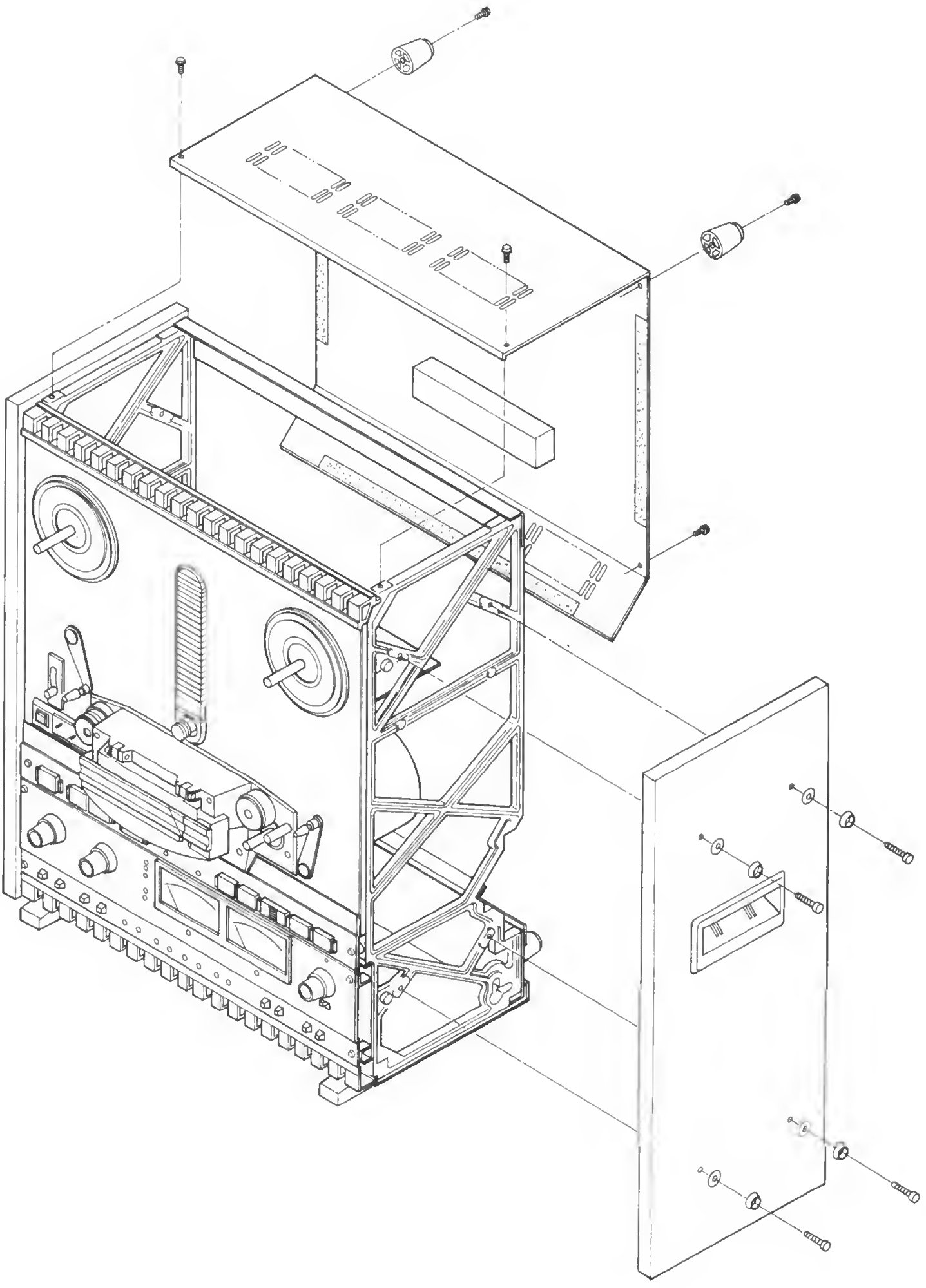
Here the access to the amplifier is described and also rear and side board panel removal is illustrated. Please refer to the illustrations on next pages.
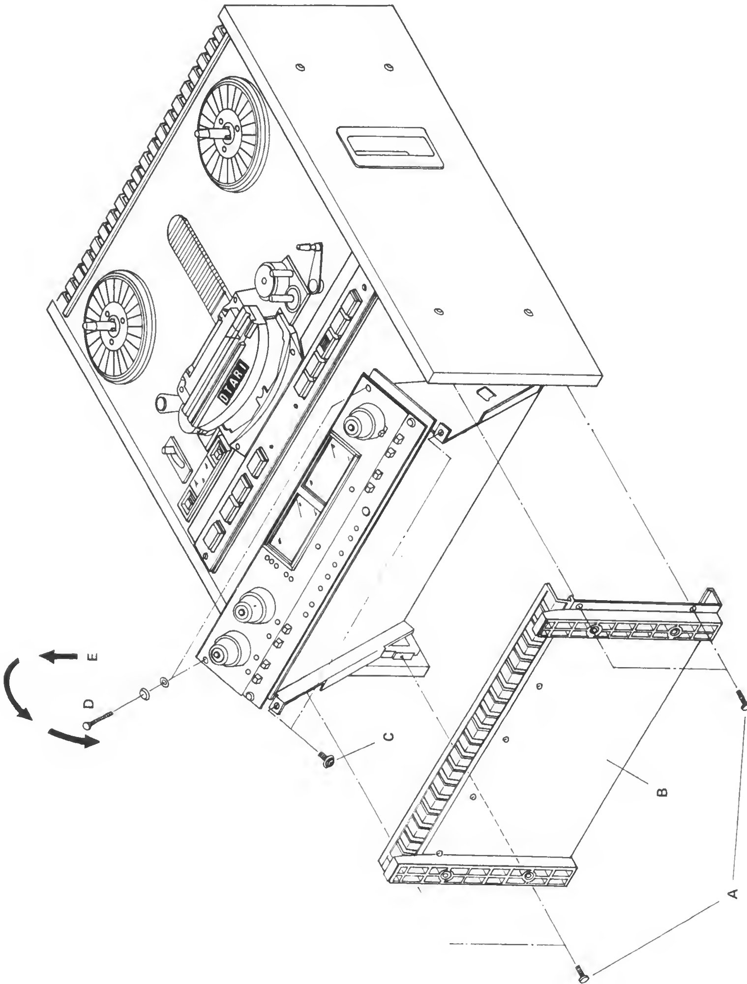
(1) Remove the 4 screws marked "A" from the bottom panel and remove the bottom panel marked "B".
(2) Remove the 2 screws marked "C" in Fig. 5-1, also remove the 2 screws marked "D". Then pull the amplifier section up and rotate it toward you.
(3) Referring to Fig. 5-3, the location of all the pots and switches are illustrated and are explained in the list following. This list would give you the convenience in adjusting the amplifier.
5.2 AMPLIFIER P.C.B. ASSEMBLY LAYOUT↑ TOP
Figure 5-3 is the major parts layout on the amplifier P.C.B. assembly with the parts list following on next page. They may give you the necessary location information of the parts to adjust the amplifier.
 ⤢ zoomIsometric exploded view of the transport tilted up with the bottom panel and rear rail assembly detached, with screws A, C, D and panels B and E called out.
Full-resolution scan of this sheet
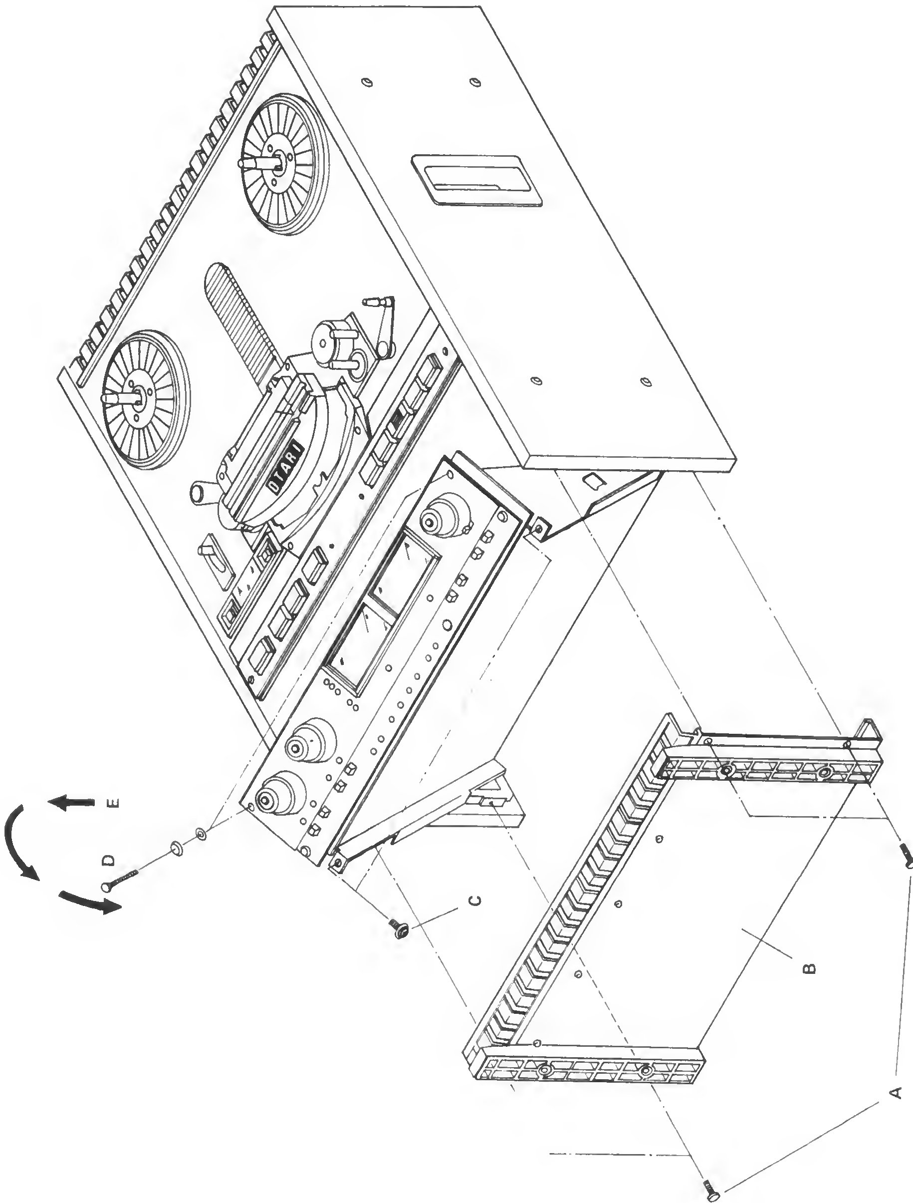
Fig. 5-1 Access to the Amplifier
 ⤢ zoomExploded view of the top cover, rear cage frame and side board lifting off the transport, with their mounting screws.
Full-resolution scan of this sheet
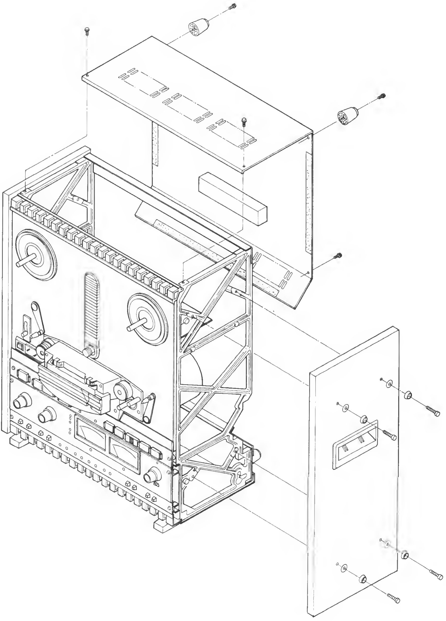
Fig. 5-2 Rear Panel and Side Board Removal
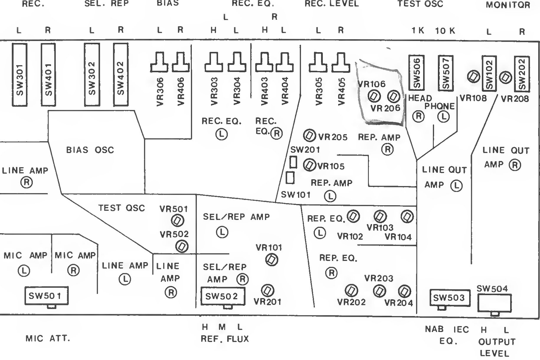 ⤢ zoomLabeled block layout of the amplifier P.C.B.'s bottom view, with switch and potentiometer designators grouped by function: record, selective reproduce, bias, record EQ, record level, test oscillator and monitor.
Fig. 5-3 Pattern Layout (bottom view)
LIST OF THE MAIN PARTS FOR ADJUSTMENT OF AMPLIFIER
Ref. No.
| SW301 | RECORD Selection LCH |
| SW401 | RECORD Selection RCH |
| SW302 | SEL/REP Selection LCH |
| SW402 | SEL/REP Selection RCH |
| SW506 | TEST OSC 1 kHz |
| SW507 | TEST OSC 10 kHz |
| SW102 | MONITOR Selection LCH |
| SW202 | MONITOR Selection RCH |
| SW501 | MIC ATTENUATOR |
| SW502 | RECORD LEVEL Selection |
| SW503 | EQ (NAB or IEC) Selection |
| SW504 | OUTPUT LEVEL Selection |
| VR306 | BIAS Adjustment Pot LCH |
| VR406 | BIAS Adjustment Pot RCH |
| VR303 | RECORD EQ Pot LCH High Speed |
| VR304 | RECORD EQ Pot LCH Low Speed |
| VR403 | RECORD EQ Pot RCH High Speed |
| VR404 | RECORD EQ Pot RCH Low Speed |
| VR305 | RECORD LEVEL LCH |
| VR405 | RECORD LEVEL RCH |
Ref. No.
| VR106 | SRL LEVEL (REP) LCH |
| VR206 | SRL LEVEL (REP) RCH |
| VR108 | SOURCE LEVEL LCH |
| VR208 | SOURCE LEVEL RCH |
| VR501 | 10 kHz TEST OSC LEVEL |
| VR502 | 1 kHz TEST OSC LEVEL |
| VR101 | SEL/REP SRL ADJ. LCH |
| VR201 | SEL/REP SRL ADJ. RCH |
| VR205 | LOW COMP. Pot RCH |
| SW201 | LOW COMP. Selection RCH |
| VR105 | LOW COMP. Pot LCH |
| SW101 | LOW COMP. Selection LCH |
| VR102 | REPRODUCE EQ Pot 15 ips LCH |
| VR103 | REPRODUCE EQ Pot 7.5 ips LCH |
| VR104 | REPRODUCE EQ Pot 3-3/4 ips LCH |
| VR202 | REPRODUCE EQ Pot 15 ips RCH |
| VR203 | REPRODUCE EQ Pot 7.5 ips RCH |
| VR204 | REPRODUCE EQ Pot 3-3/4 ips RCH |
5.3 BLOCK DIAGRAM AND CIRCUIT DESCRIPTION↑ TOP
Block diagram of the amplifier is illustrated at Fig. 5-4. Refer to this illustration and schematics on the last section of this manual for more understanding circuit descriptions.
5.3.1 REPRODUCE CIRCUIT↑ TOP
Please refer to A1062 Rec & REPRO AMP schematics on last section of this manual. All descriptions are made with the circuit terms in the schematics.
The reproduce head is connected to #9-4 and #9-3 and the signal reproduced goes to the input stage of EQ amplifier through Q105, which is the gate switching "Sel-Rep" signal and "Reproduce" signal. Sel-Rep signal comes through brake contact of the record relay to sel-rep amplifier. Sel-Rep amplifier is composed by Q101, Q102 and Q103 amplifiers and VR101 is for sel-rep level adjusting. Q104 is the same switching gate as Q105 in reproduce circuit. IC501 is an EQ amplifier with many resistors inserted to the NF circuits by means of FET switching (Q106~Q111).
IC101-1/2, VR105 and SW101 are for low frequency compensation circuit. The equalized reproduced signal is transferred to the other half of IC101 through VR106, NORMAL-SRL switch and MONITOR switch. VR106 is SRL adjusting potentiometer and VR107 is output level adjusting potentiometer on the front amplifier panel. Reproduce signal line is grounded through R139 and Q112 at hot end of VR106. The base of Q112 is driven by FAST command, which mutes the audio signal during FAST WINDing.
The audio signal selected by monitor switch is supplied to PEAK indicator circuit and pre-output amplifier. The amplitude gain of this amplifier is decided by R147~149 and two transistors to which control command is running through record level selecting switch, SW502-b.
The output of pre-output amplifier goes to phones amplifier circuit and active balance line out circuit. And also it is connected to emitter of Q115 which is final stage of power-on muting circuit. IC102, IC103 and Q117~Q120 are for active balance circuit which is connected to the output XLR connector.
5.3.2 RECORD CIRCUIT↑ TOP
There are two input circuits in the record amplifier. One is MIC INPUT and the other is LINE INPUT. Both are active ballance circuits. MIC input signal is output to VR301 which is MIC level potentiometer on the Amplifier front panel. Also LINE input signal is output to VR302 which is LINE level potentiometer on the panel. Q301 and Q302 are inserted before the VR302. Both
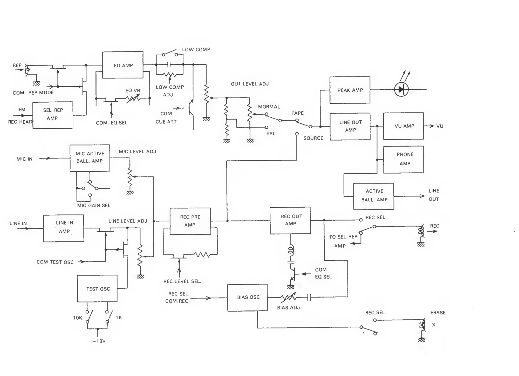 ⤢ zoomFull amplifier block/signal-flow diagram, from the mic, line and test oscillator inputs through the equalizer, bias oscillator and output stages to the erase, record and reproduce circuits.
Full-resolution scan of this sheet
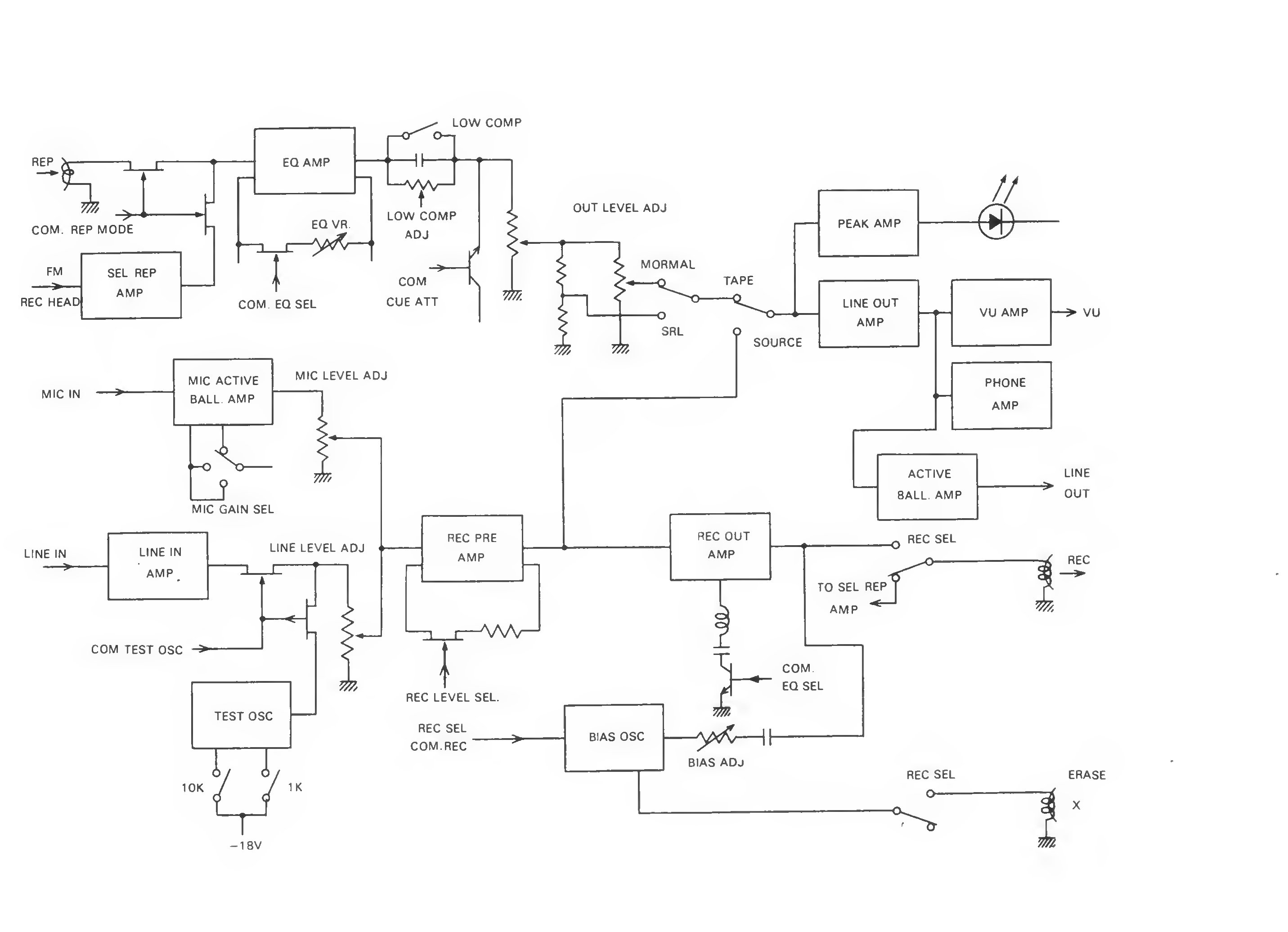
Fig. 5-4 Block Diagram
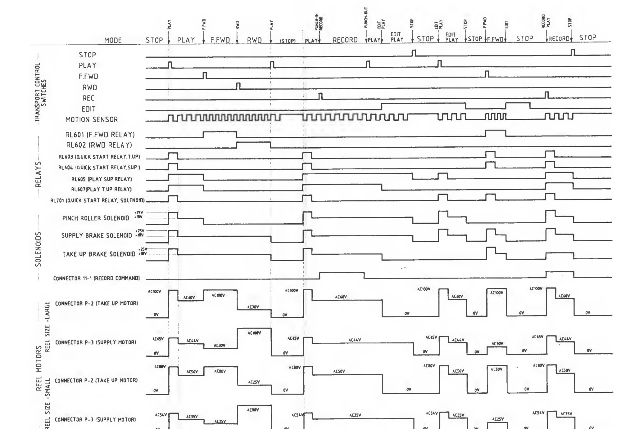 ⤢ zoomTransport control timing chart, showing the mode switches, motion sensor, relays, solenoids and reel motor AC voltages against STOP, PLAY, fast forward, rewind, record and edit modes.
Full-resolution scan of this sheet
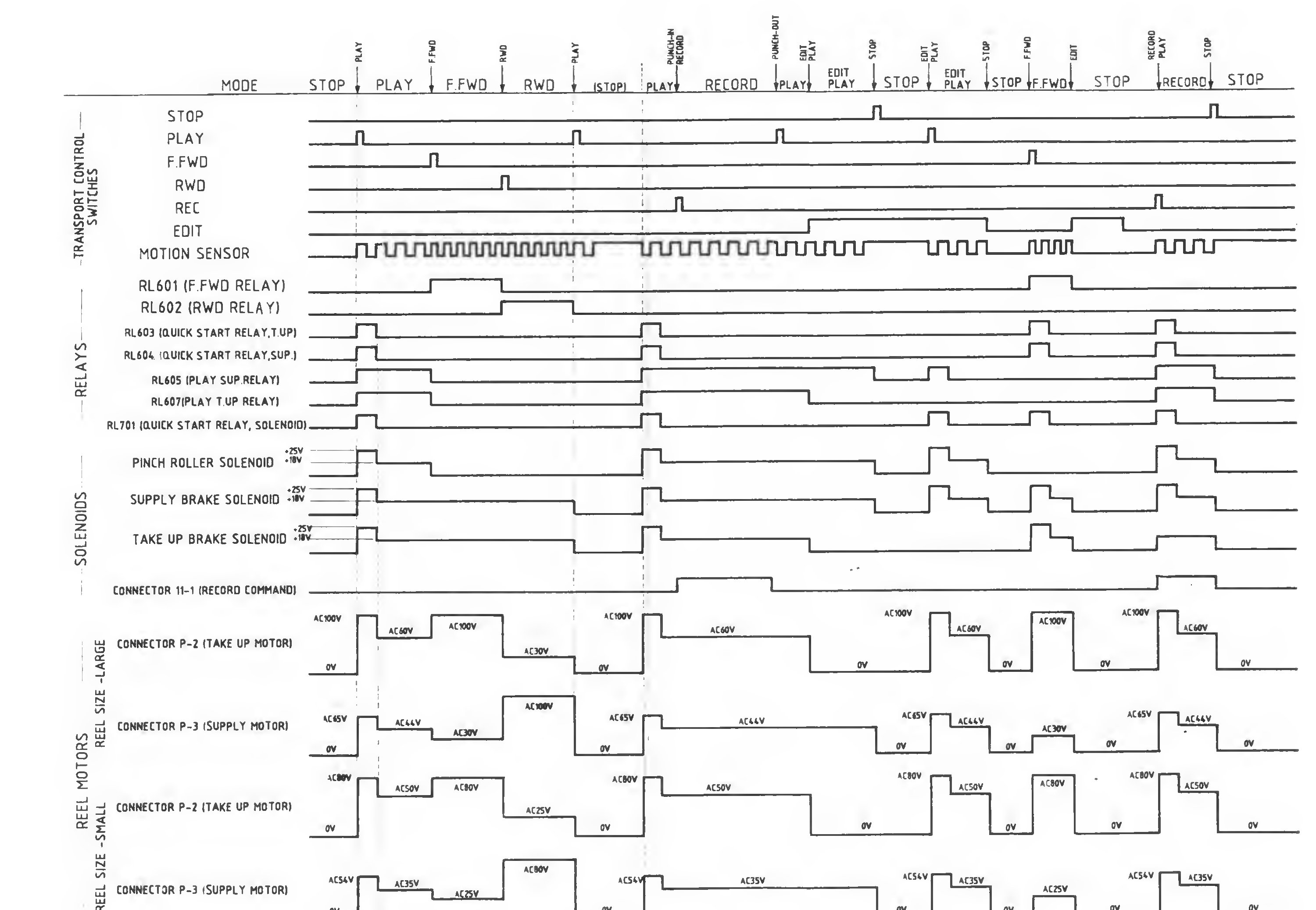
Fig. 5-5 Transport Control Timing Chart
transistors are switching gates to feed 1 kHz or 10 kHz sine-wave signal to the line amplifier. Then both input' signals are mixed together at the input stage of line pre-amplifier IC505. Its gain is also controlled by record level selecting switch SW502-b.
IC302 with 3 FET's Q305 ~306 makes half of the record EQ circuit and VR305 is for record level adjustment. Then record signal is supplied to other half of the record EQ circuit composed with IC302, Q313 ~Q317 and many EQ components. The output of the record EQ circuit is fed to the output stage of BIAS oscillator through bias trap circuit composed with L301 and other CRs.
Bias circuit is composed by Q509, Q510 and T501. Full output of bias circuit is fed to erase head and its tapped output is fed to record head through VR306 and C320. VR306 is a bias adjusting potentiometer. L302 is a dummy load for the compensation in the case of single channel recording. DC voltage for bias oscillation circuit is fed through voltage control circuit, Q504 ~508. Those are for click-less recording. IC506 and many C-R components are for sine-wave test oscillator circuit.
5.4 TRANSPORT CONTROL TIMING CHART↑ TOP
Fig. 5-5 is a transport control timing chart of MX-5050BII. All control timings are shown in the chart including record command.
5.5 AMPLIFIER ADJUSTMENT↑ TOP
Here amplifier adjustment is well described in order from test tape selection to record EQ adjustment. There are short descriptions on amplifier adjustment and locations and functions of each potentiometer and other stuffs for adjustment at Section IV. So please refer to Section IV also.
5.5.1 TEST TAPE SELECTION↑ TOP
MX-5050BII Series are adjusted with the standard test tapes listed in the table below. We recommend you to use the same type of standard test tapes.
Table 5-1 Reproduce Alignment Test Tape
| Tape Speed | Equalization | MRL Catalog Number | Reference Level |
|---|---|---|---|
| 15 ips | NAB | 21J205 | 250 nwb/m *1 |
| 7-1/2 ips | NAB | 21T204 | 250 nwb/m *1 |
| 3-3/4 ips | NAB(=IEC) | 21F101 | 200 nwb/m *1 |
| 15 ips | IEC | 21J303 | 320 nwb/m *2 |
| 7-1/2 ips | IEC | 21T302 | 320 nwb/m *2 |
*1 Short circuit flux density *2 Open circuit flux density which corresponds to 290 nwb/m in short circuit flux density
5.5.2 HEAD ALIGNMENT↑ TOP
(1) Figure 5-6 shows head assembly of the MX-5050BII. Each head unit is supported with three screws and springs to the head mounting plate.
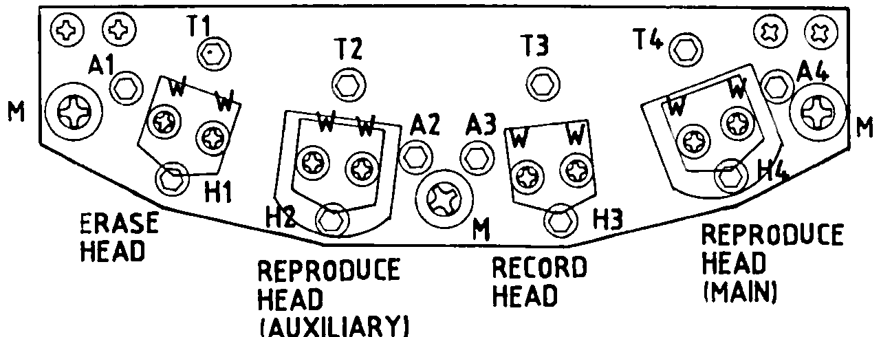 ⤢ zoomLine-art diagram of the head-mounting plate with mounting-screw callouts M, T1-T4, A1-A4, H1-H4 and W, and the erase, reproduce (auxiliary), record and reproduce (main) heads labeled.
Fig. 5-6
(2) When replacing a whole head stack, take out three screws marked M in the figure.
(3) When replacing only a head unit, take out three screws marked Tn, An and Hn of the head.
(4) When new head unit or new head stack is mounted, first roughly adjust the height of the head with the tape thread as illustrated in Fig. 5-7. To adjust the height turn three screws by same amount.
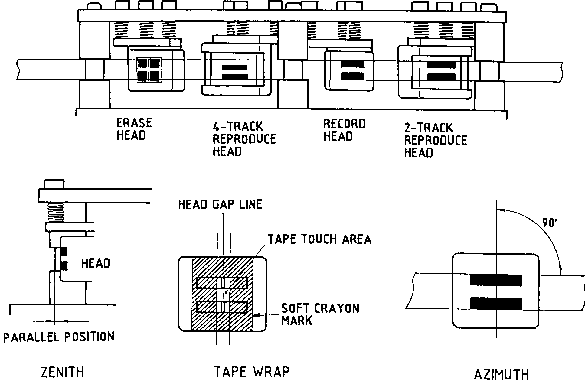 ⤢ zoomLine-art diagram of the four tape heads in cross-section, with the head-mounting screw's parallel position, tape wrap and azimuth angle illustrated below.
Fig. 5-7
(5) Then paint the head face with a soft crayon or marking pen, run the tape for about ten seconds, and check the trace of the tape. If head adjustment is correct, the shape of tape touch area on the head should be rectangular and should be equal shape to the head gap line as illustrated Fig. 5-7.
(6) To have those results, adjust and check the zenith, tape wrap and azimuth of the head with five screws as explained on the Table 5-2.
Table 5-2
| Height Adjustment | "A", "T" and "H" | Turn the screws by same amount. |
| Zenith | "T" or "H" | Check the height at the same time. |
| Azimuth | "A" | Refer to 5.5.3. |
| Tape wrap | "W" | Loose both screws, and twist the head. Then tighten the screw again. |
(7) Through steps (1) to (7), head mounting is roughly adjusted. Following adjustments are necessary whenever the head or head assembly is replaced. So refer to next 5.5.3 for further fine adjustment with a test tape and a blank tape.
-
Reproduce head replacement
A. Reproduce EQ adjustment
B. SRL adjustment -
Record head replacement
A. Record bias adjustment
B. Overall frequency response adjustment
C. Record level adjustment -
Erase head replacement
Erase current measuring
5.5.3 REPRODUCE EQUALIZATION ADJUSTMENT↑ TOP
(1) Prepare the tape deck for reproducing the test tape as instructed in Table 5-3. Thread low speed test tape first. Head azimuth adjustment should be done at lower speed of the machine.
Table 5-3
| Switch | Switch Position | Note |
|---|---|---|
| RECORD SELECTOR | OFF | |
| SEL-REPRO | OFF | |
| MONITOR | TAPE | both channel |
| REF FLUX | MID | for 250 nwb/m test tape |
| EQUALIZATION | NAB | or IEC |
| SRL SWITCH | ON (SRL) | |
| OUTPUT LEVEL | HIGH | for +4 dBm OUTPUT |
| TAPE SPEED | LOW |
(2) Put the tape deck in PLAY mode and reproduce reference level section of the test tape and adjust VR106 (SRL LEVEL) to read 0 VU on the VU meter.
(3) Observe the line output with a dual trace oscilloscope during reproducing 10 kHz or higher frequency section of the tape. Adjust A4 screw to have correct phase shift as illustrated below.
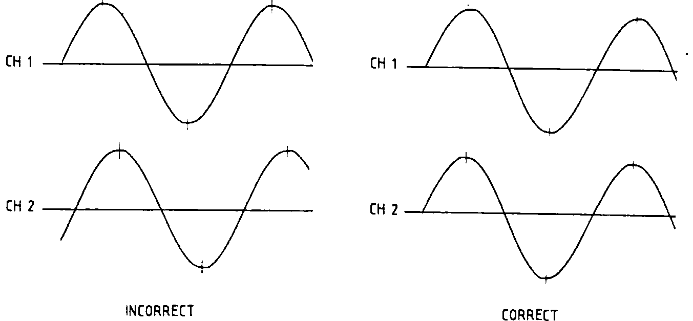 ⤢ zoomTwo pairs of stacked sine-wave traces, labeled INCORRECT (left pair) and CORRECT (right pair), illustrating phase-shift adjustment on channels 1 and 2.
Fig. 5-8
(4) When correct phase shift adjustment has been done, then adjust VR103 to have flat frequency response. After this adjustment, reproduce reference level section again and check if 0 VU adjustment held at step (2) is drifted or not. If drifted adjust VR106 again.
(5) Do the same steps (3) and (4) at higher speed with high-speed test tape.
5.5.4 BIAS ADJUSTMENT↑ TOP
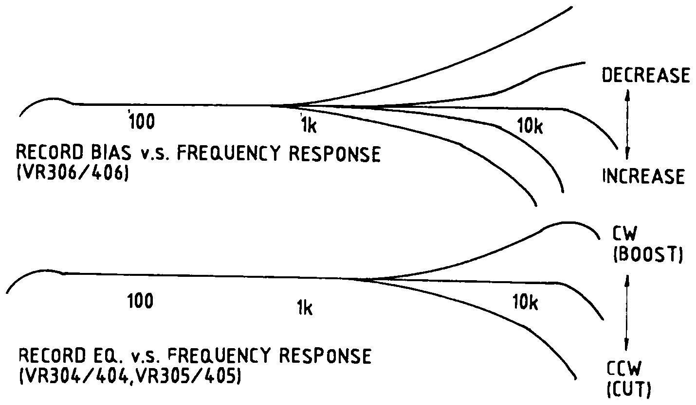
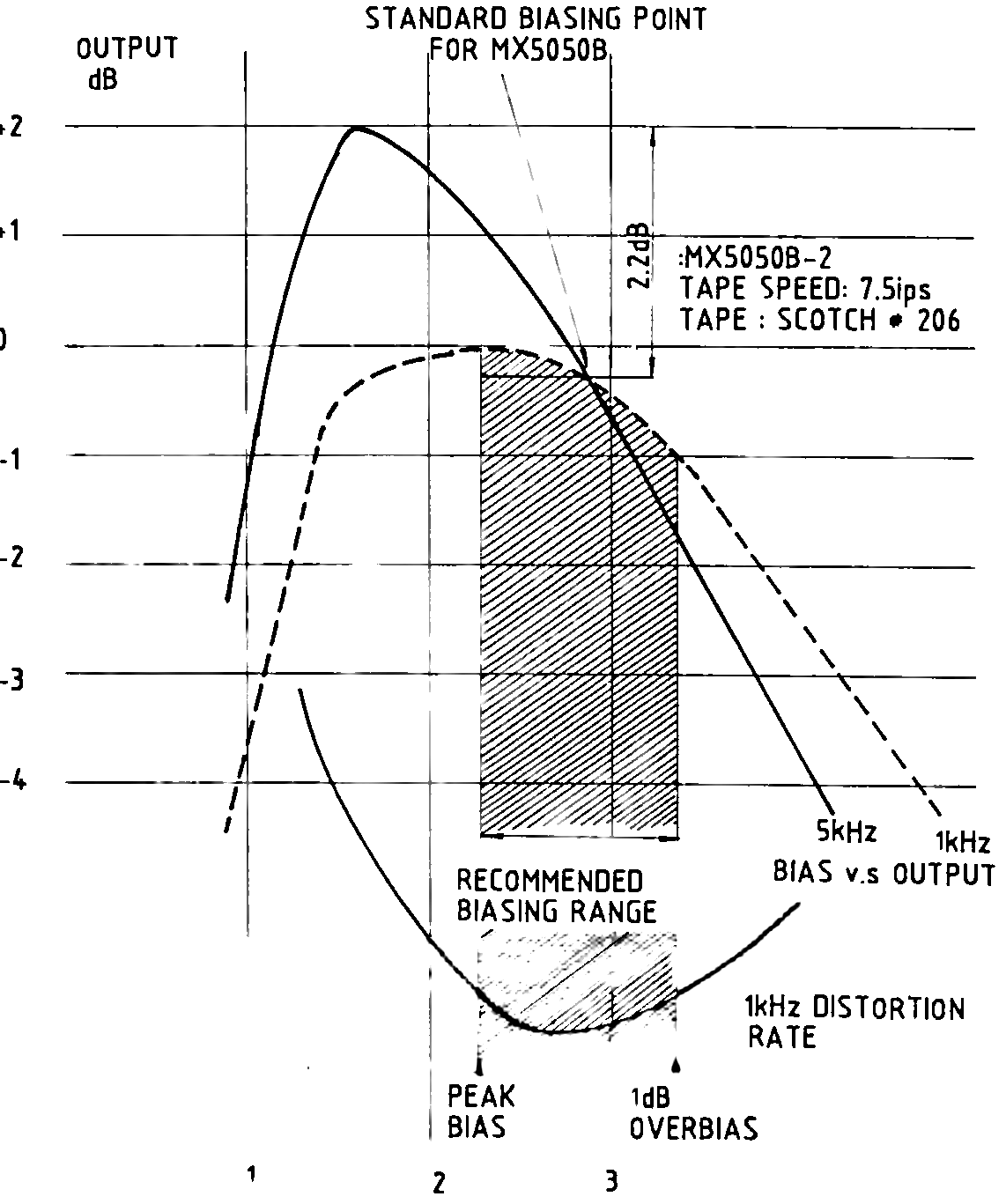
Figure 5-9 shows the variation of the frequency response by the bias set and the Record EQ adjustment control, and Fig. 5-10 shows the characteristics of the output and distortion vs. bias current.
 ⤢ zoomTwo frequency-response curve charts stacked vertically: record bias versus frequency response with a decrease/increase arrow, and record EQ versus frequency response with a CW (boost)/CCW (cut) arrow.
Fig. 5-9
 ⤢ zoomChart of output and distortion versus bias current, with a standard biasing point callout, a recommended biasing range band, and peak bias and 1 dB overbias marks.
Fig. 5-10
The amount of the bias current relates to the distortion and the overall frequency response. So overall frequency response may be adjusted with both the record EQ and the bias current adjustment for a flat frequency response. Normally record bias should be set between the peak bias and some amount of over bias at 1 kHz for lower distortion and high maximum output.
(1) Feed 1 kHz, 0 dBm signal to input of the recorder. Monitor the input and adjust input level control knob to read 0 VU on the VU meter. Then set the MONITOR switch to the TAPE position. Select SRL position of the SRL switch.
(2) Put the machine in RECORD mode at 15 ips.
(3) Turn down (counterclockwise) the bias control potentiometer once and gradually turn it up clockwise. The VU meter reading will increase. Find out the peak point of the output level as explained with Fig. 5-10.
(4) Feed 10 kHz signal and adjust screw A3 to have same phase relation as explained previously at reproduce head adjustment.
(5) When head adjustment has been completed, adjust VR303 (L ch in 15 ips) to have 0 VU reading on the VU meter.
(6) Change input signal frequency from 30 Hz to 20 kHz and check if frequency response is within specification. Adjust Record EQ pot and bias if necessary.
(7) Do the same steps for the record frequency response at lower tape speed. In this case input signal level should turn down by 10 dB, so recording should be held at -10 VU output.
5.5.5 RECORD LEVEL, MONITOR LEVEL ADJUSTMENT↑ TOP
(1) Set SRL select switch to SRL.
(2) Feed -15 dBm, 1 kHz sine-wave signal to input. Turn the input level control knob all the way up.
(3) Put the machine into Record mode and monitor off the tape.
(4) Adjust VR305 to have 0 VU reading on the VU meter.
(5) Then select the "SOURCE" position of the monitor switch.
(6) Adjust VR108 to have 0 VU reading.
5.5.6 PEAK INDICATOR TRIGGER LEVEL ADJUSTMENT↑ TOP
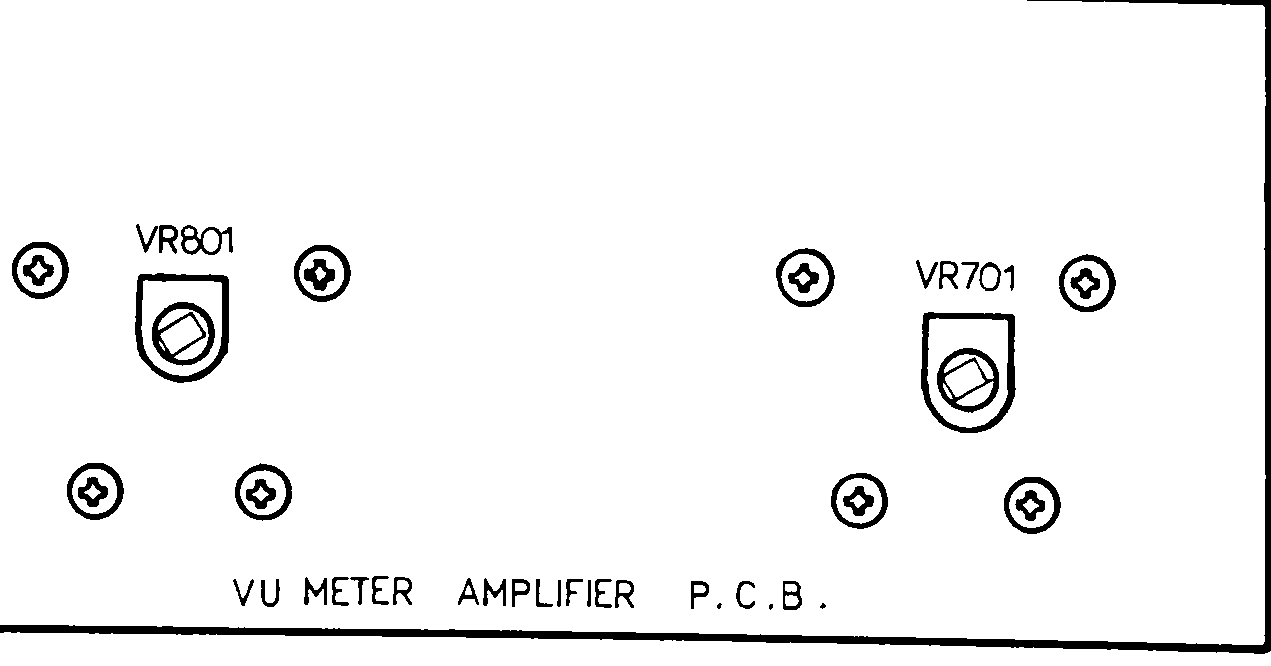
Peak indicators are triggered at the recorded flux level of 520 nWb/m. This point is 9 dB above 185 nWb/m (RECORD LEVEL switch in "L" position), 6.4 dB above 250 nWb/m (RECORD LEVEL switch in "M" position), and 5.2 dB above 320 nWb/m (RECORD LEVEL switch in "H" position as shown in Fig. 5-11.
 ⤢ zoomRectangular line-art board outline of the VU meter amplifier P.C.B., with potentiometers VR801 and VR701 and their mounting screws called out.
Fig. 5-11 VU Meter Amplifier P.C.B.
For peak indicator trigger level adjustment, proceed as follows:
(1) Set the RECORD switch to the "L" position, connect the audio oscillator to the LINE INPUT terminals, and feed a 0 dBm signal.
(2) Set the MONITOR switch to the SOURCE position and adjust the LINE INPUT controls for a 0 dB indication on the VU meter.
(3) Shift the feeding level of the audio oscillator to +9 dBm.
(4) Turn the VR701/801 adjustment controls on the VU meter amplifier P.C.B. fully counterclockwise and then clockwise until each peak indicator in the VU meter illuminates.